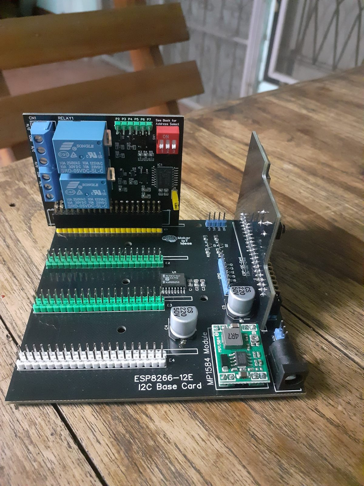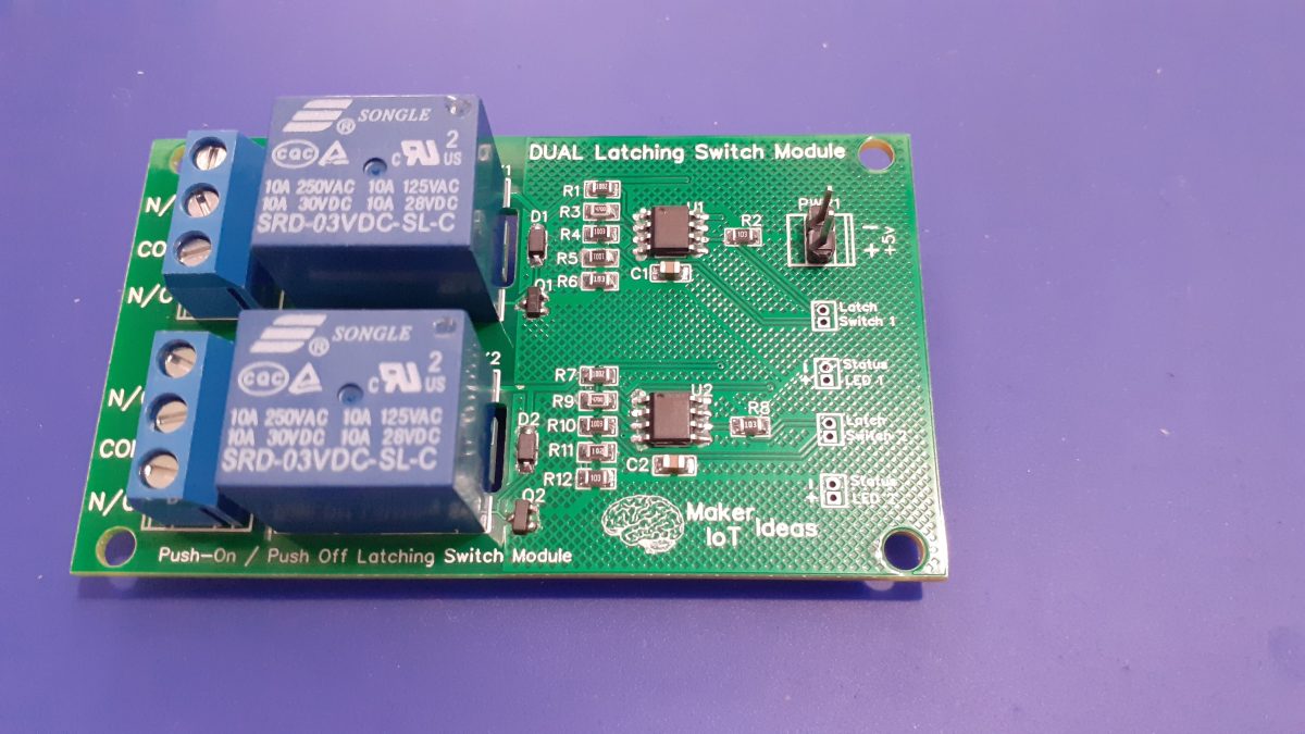
In a recent post, I looked at a single-channel version of this module. While it may be a repetitive post, I will continue, as it shows how easy it is to double up on this circuit to provide more than one latching switch on a single circuit board. The current drawn by this module is so little, even when energised, that it compares favourably with even a microprocessor-controlled solution.
The real advantage will obviously be the cost, as the hand full of discrete components needed for this is way cheaper than a microprocessor alone, and the fact that it doesn’t need any coding makes for an attractive solution.
It is however worth noting that the circuit is quite sensitive to external interference, sometimes resulting in unwanted operation. This does not concern me too much, as 1) This is still a prototype and 2) While it does work as intended, and surely is quite useful, I do not intend using it to switch any high current load, or control any expensive or important equipment.


Since the previous post looked at the base circuit in detail already, I think it will be a good idea to talk a bit about electrical isolation, tracking and keeping the AC and DC sides of a circuit separated completely

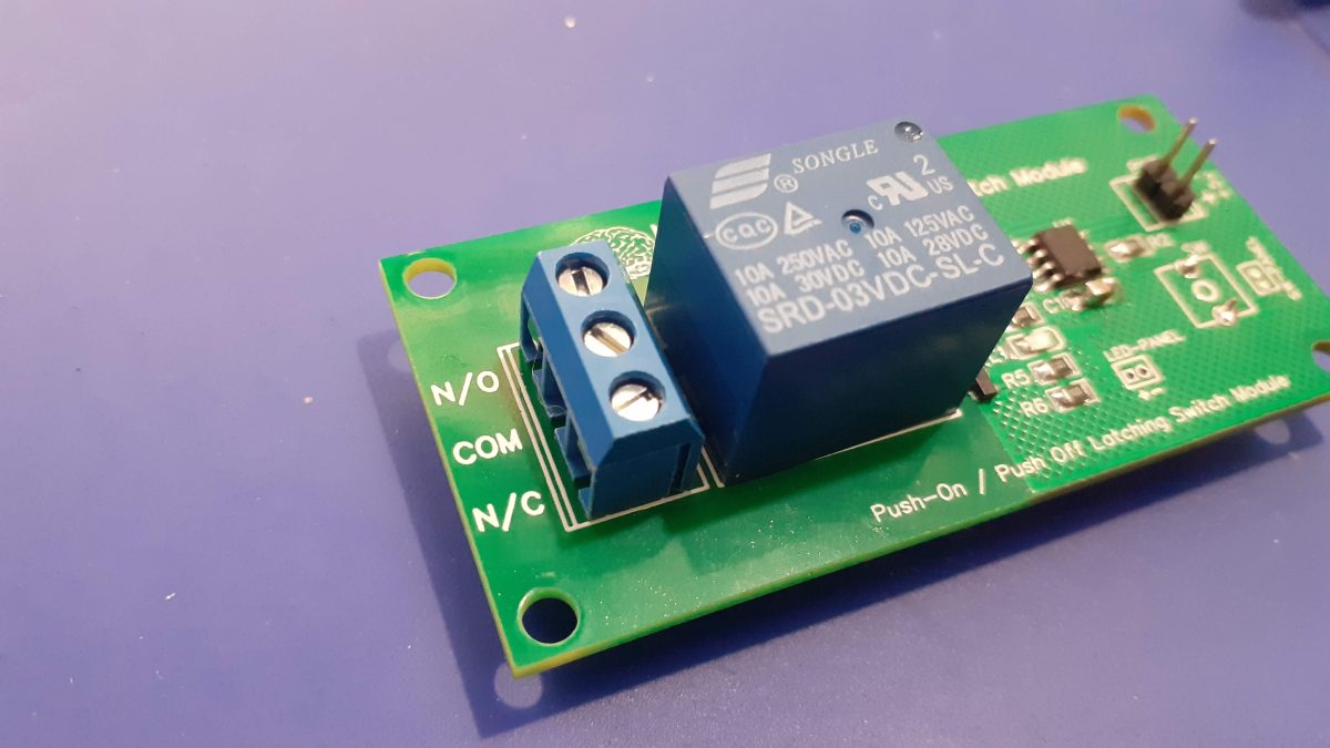
In the picture above, we can clearly see that the DC side (near my hand, at the top is contained completely on the right side (top in this case) of the PCB. The hashed copper pour also stops clear of the two relays. There are only four tracks
going to the relay coils, and they are all on the same layer of the PCB.
Also note the square cut-out slot around the common terminal of each of the relays. This provides additional isolation to the relay, as well as the DC side of the circuit, as air is a very good insulator ( at least for 220v at no more than 10A — or so I was taught …) These cutouts will prevent any mains voltage of tracking, think burning towards, towards any other tracks in this area.
The entire left-side top layer ( underneath the relays) are also completely free of copper, to make tracking even more difficult.

If we now look at the bottom layer of this same PCB, we will see that the DC side and its ground-plane are once again completely separated from the relay contact terminals. Also note that the tracks connecting the screw-type connector and the relay terminals are very thick (100mil), straight and as short as possible. All copper around these tracks has also been etched away, further reducing the chances of tracking.
In a production PCB, Warning labels would also be present in the bottom silkscreen of the PCB in this area, warning the user of the possibility of mains voltage in this area. As this is a prototype, and to make the above-mentioned points easier to see, I have not added these labelling on these boards.
Important Disclaimer:
Electricity is NEVER “SAFE”. There are only safe practices and procedures. It is always the responsibility of the user to ensure their own safety. While the design shown above is considered “SAFE” by myself, I only consider it “SAFE” because I am aware of the risks involved in using such a circuit to switch mains voltage, at a certain current, and under a specific use scenario. DO NOT BE FOOLED into simply replicating this circuit, or parts of it, and believing it is “SAFE”. Every use case of a circuit is different, and the devices connected and controlled by it will always differ. Make sure that you ACTUALLY know what you are doing BEFORE using any High voltage/Current and switching it with any electronic device.
Manufacturing
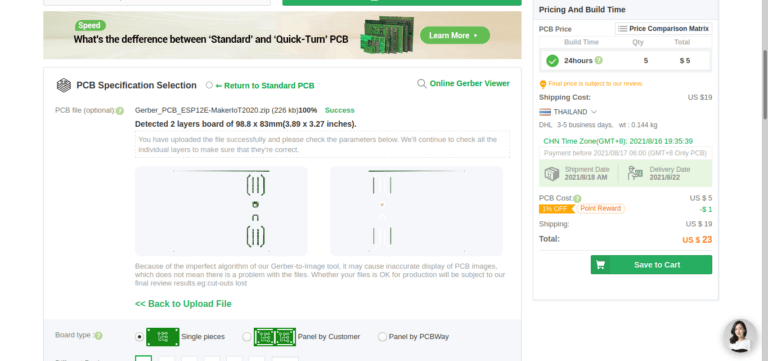
The PCB for this project has been manufactured at PCBWay.
Please consider supporting them if you would like your own copy of this PCB, or if you have any PCB of your own that you need to have manufactured.

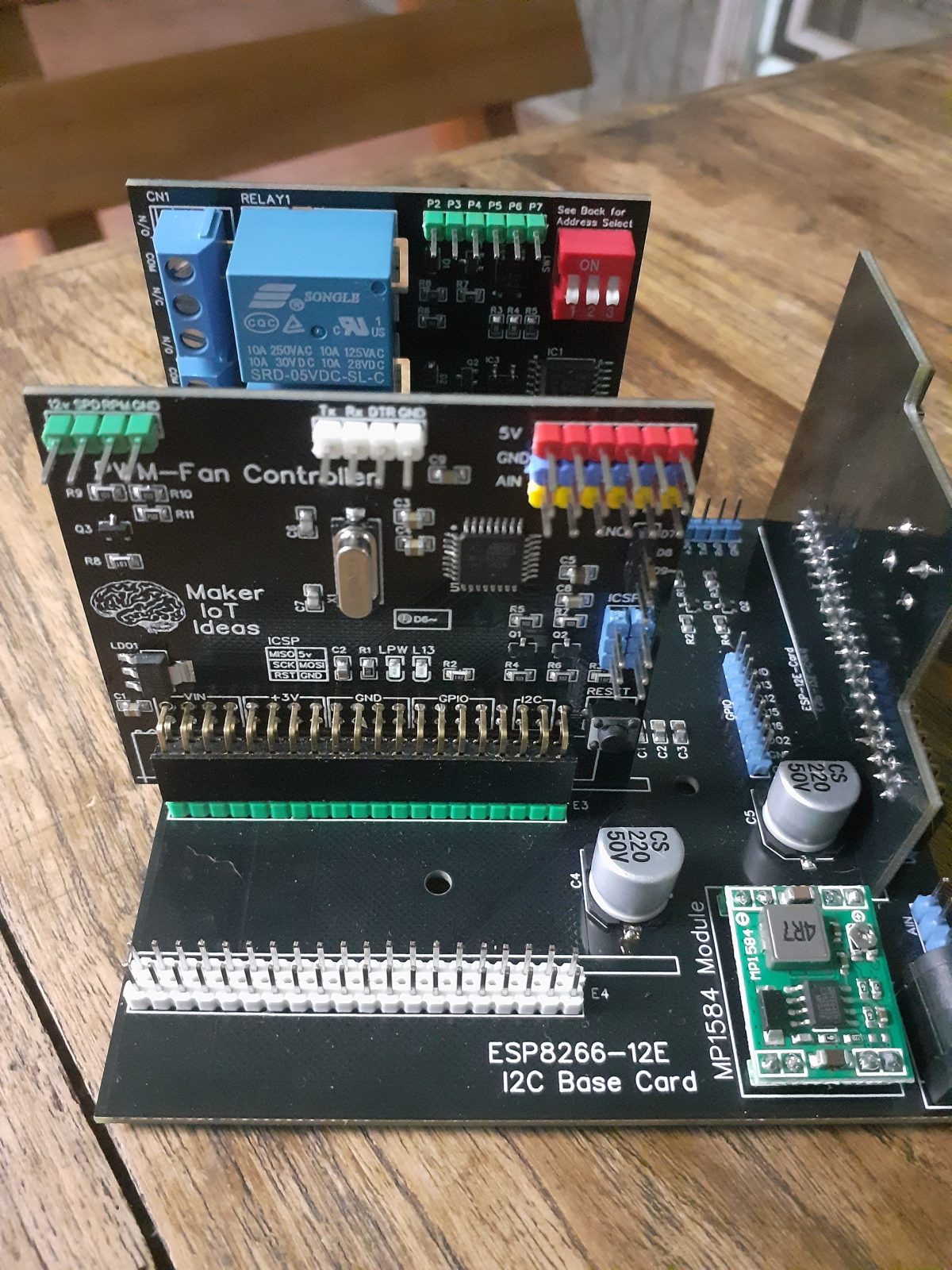
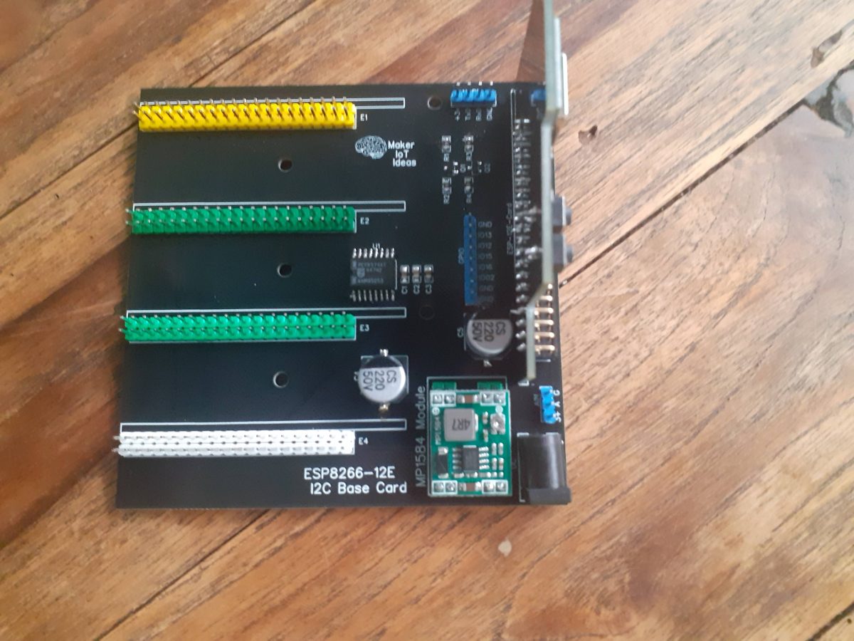
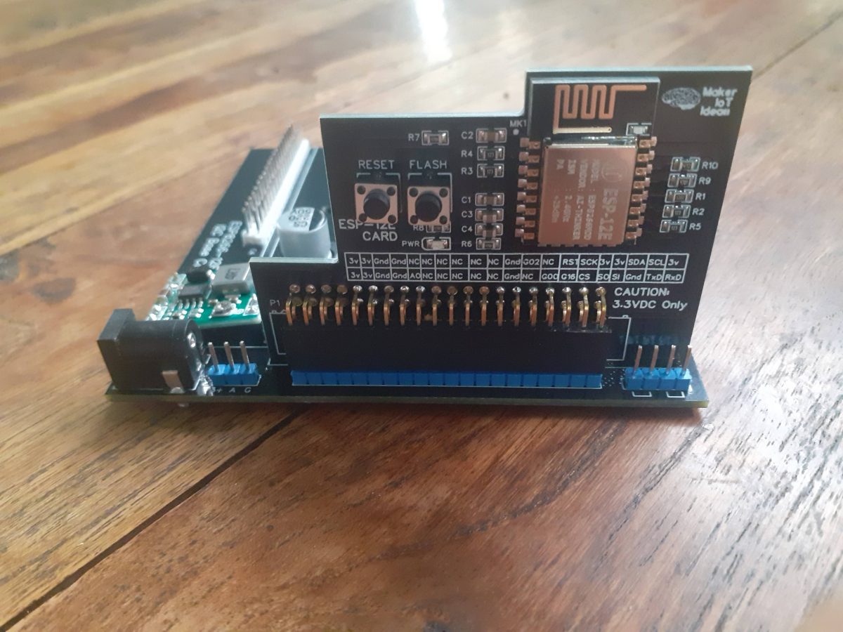
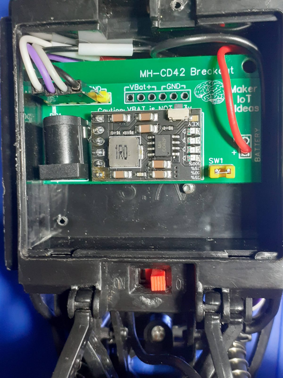
Some More Pictures