While prototyping our projects, we Makers often need to interface devices with a higher current draw, like motors, or RGB lights, to our microcontrollers. These typically are unsuitable for connecting directly to an Arduino, ESP32 or Raspberry Pi’s GPIO pins. This is usually the time when we start grabbing transistors or MOSFETs.
While I normally keep a few leaded transistors and MOSFETs in the lab, These are not always convenient to use, as they may be in big packages or have the wrong specifications for the task that we are trying to perform.
SMD versions are more common in my lab, but they come with the problem of being small, and also completely unfriendly to the breadboard environment.
I have thus been playing with an idea to make a series of dedicated breakout boards for just this purpose. Having an easy way to test a specific MOSFET for a design, and having more than one of them handy, without all the wiring issues, and using the bare minimum of those DuPont wires!
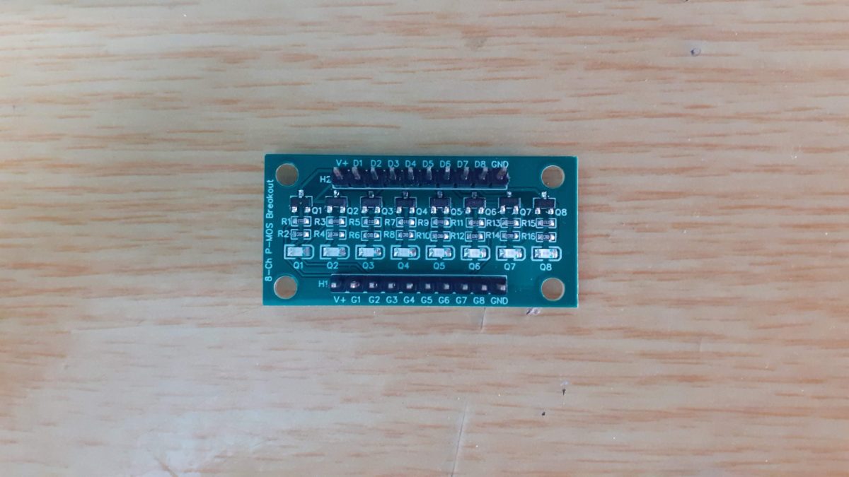
I came up with the following prototype, which, while not completely optimised yet, already makes things easier. The breakout board provides 8 P-Channel Mosfets, with a single source connection, and individually broken-out Drain and Gate pins.
LED indicators on each channel provide a visual indication of the status of each P-Mos device, and the breakout can also be mounted directly into an enclosure if needed.
What is on the PCB?
Each channel comprises a P-Channel Mosfet, in this case, a SI2301, which has a suitably low gate voltage, a pullup resistor on the gate, to keep it from floating, a status-indicating LED and a current-limiting resistor for the LED.
No gate resistor was added, as this would change depending on the actual MOSFET, as well as the microcontroller that you use. The Gate pullup resistor can also be left unpopulated, in case you need to do something specific there.
Two rows of 10-way, 2.54 header pins are at the top and bottom of the PCB, to make using the breakout on a breadboard possible.
The Pinouts are as follows
H2 – Top V+ D1 D2 D3 D4 D5 D6 D7 D8 GND with Dx corresponding to the Drain pin of each MOSFET. All the Source pins are internally connected together, as I assumed that I will use the same source voltage on each channel anyway.
H1 – Bottom V+ G1 G2 G3 G4 G5 G6 G7 G8 GND with Gx corresponding to the gate pin of each MOSFET.
V+ and GND for each header is internally connected, to make it possible to supply V+ and Gnd on any of the two headers.
PCB Top Layer
The Schematic
Schematic
Using the Breakout
Using the breakout is straightforward. Connect a source voltage to either of the V+ pins and Ground to either of the GND pins. ( the ground is used internally for the status LEDs)
Connect your load, with the positive to a drain pin, let us say D1, and the load ground to your breadboard, or power supply ground. Connect the corresponding gate pin, in our case G1, to the microcontroller pin of your choice, through a suitable gate resistor, and pull it high at setup, to ensure that the MOSFET stays off. Pull low to activate as needed.
Please note that you should not try to switch excessively large currents through a single MOSFET Channel, as the PCB traces can realistically only handle approximately 300 to 400mA per channel.
Note 2: If you are driving an inductive load, it is considered good practice to add a flywheel diode on the load as well. This will protect the MOSFET from back EMF when the MOSFET is switched off.
PCB Back
Manufacturing
The PCB for this project has been manufactured at PCBWay. Please consider supporting them if you would like your own copy of this PCB, or if you have any PCB of your own that you need to have manufactured.
Example code for using the breakout (Arduino)
// Declare Gate driving GPIO pins
int gate1 = 10;
int gate2 = 11;


void setup() {
// Set the GPIO pins as outputs and drive them HIGH
// This keeps the channels switched "OFF"
  digitalWrite(gate1,HIGH);
  digitalWrite(gate2,HIGH);
  pinMode(gate1,OUTPUT);
  pinMode(gate2,OUTPUT);

// Writing to the GPIO's before setting their pin Mode,ensures that the
// GPIO's are in fact initiated in a know correct state.

  Serial.begin(115200);

}

void loop() {
// In the loop, we just toggle the GPIOs, thus
// alternatively switching the channels on or off
  digitalWrite(gate1,!digitalRead(gate1));
  digitalWrite(gate2,!digitalRead(gate1));
  delay(1000);
  }
This post will look at my prototype Analog front-end for the Scoppy RP2040 Oscilloscope. It is important to state right from the beginning that this circuit is one of the 5 recommended designs from the Scoppy Website. I have only moved it from the breadboard design as published, onto a PCB.
The entire circuit, with all of the original designer’s writeups, is available here
So, why use someone else’s circuit? Well, the reason for this is two-fold. 1) The circuit designer also designed the firmware, so it stands to reason that his circuit will be optimised for use with the firmware. 2) Using his circuit provides a solid reference, making it possible to test the firmware for correct operation, and later on, providing a base for my own design – if and when I do decide it is worthwhile to actually design my own.
As I already have a proper oscilloscope as well as a logic analyser, this entire exercise is purely academic, I find the Scoppy project interesting, and as such, I would like to see how it compares with my commercial products ( while also knowing that it won’t be a very fair comparison ).
With all the limitations, I am however still quite impressed at the level of use that you can get out of this very simple device. It is definitely quite useful for a beginner.
What is on the PCB, and what did I change?
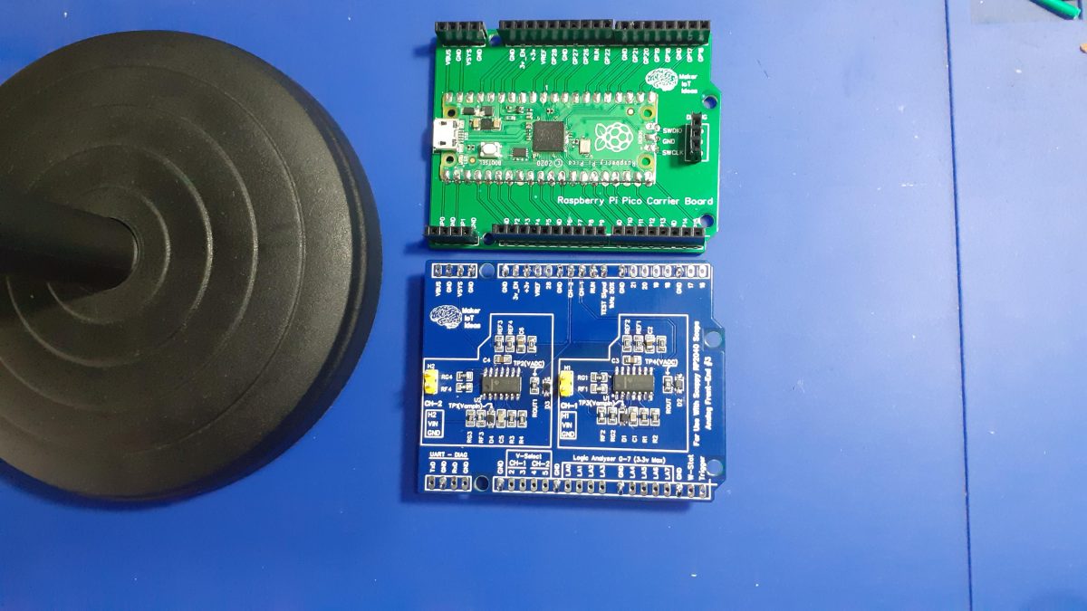
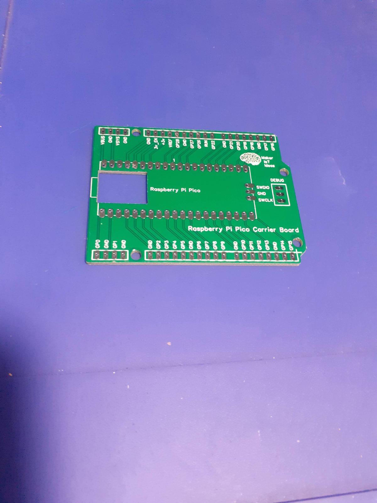
The PCB is a dual-layer shield that is designed to be used with the MakerIOT2020 Raspberry Pi Pico Carrier board. The shield is directly powered by the carrier board.
The original Analog Front-End #3 circuit featured a single channel input, capable of accepting a -18.0v to 18.0v signal input.
My changes were limited to doubling up on that circuit, to provide two channels.
I have redrawn the original schematic, partly to make it easier to understand for myself, as well as to help me with the design of the PCB.
Lets take a look at the schematic ( by using text from the original designer) The author makes no warranty, representation or guarantees regarding the suitability of this design for any particular purpose. Nor does the author assume any liability arising out its use and specifically disclaims any and all liability, including without limitation special, consequential or incidental damages.
This design builds on Design 2 and adds over and under voltage protection to the analog front end. After all, we won’t have a cheap oscilloscope if we keep frying our components!
I’m assuming here that the minimum and maximum voltages that will be applied to the input of the scope will be -18V and +18V respectively. It has been tested from -18.5V to 18.5V (two of my 9V batteries in series) but of course If you decide to use this design you are doing so at your own risk. I personally wouldn’t use Scoppy with an expensive phone/tablet just in case something unexpected goes wrong (better to use an old, obsolete phone that is no longer used for anything else) – especially when dealing with higher voltages – but of course you can do what you like.
Protecting the Op-Amp input(s)
First of all we need to protect the op-amp. In this design we’ll be using an LM324 op-amp, which is very similar to the LM358 but contains four individual op-amps rather than two. We’ll be using three of these op-amps. The reason for this will be explained later.
According to the datasheet for the LM324 the allowed input voltage range goes from -0.3V to 32V. Of course 32V is above the maximum expected voltage (18V) and so we don’t need to worry about over-voltage protection. However we do need to ensure that the voltage at the input pins don’t go below -0.3V. A schottky diode can be used to clamp the voltage to something above -0.3V (D1 in the schematic).
One thing that needs to be considered when selecting the diode is its reverse current. The 1N5817 has a very low forward voltage but high reverse current and this results in a voltage drop at the input of the op-amp (in the order of 100mV). Presumably this is because it draws current through the high value input resistor (Rg1). The 1N5711 has a much lower reverse current specification and I couldn’t discern any voltage drop when this was inserted into the circuit. However, its forward voltage (at the current expected in this part of the circuit) is very close to the minimum allowed voltage of -0.3V. To be safer I prefer to use something like a BAT46. It does result in a voltage drop of a few millivolts but the clamped voltage is more like -0.23V.
Protecting the Pico/RP2040
The Pico datasheet states that:
the ADC capable GPIO26-29 have an internal reverse diode to the VDDIO (3V3) rail and so the input voltage must not exceed VDDIO plus about 300mV
The obvious way to protect the ADC inputs (GPIO26-29) then is to simply insert a schottky diode between the ADC input and VDDIO. However, the RP2040 datasheet says that:
the voltage on the ADC analogue inputs must not exceed IOVDD ...<snip>... Voltages greater than IOVDD will result in leakage currents through the ESD protection diodes
That suggests to me that we shouldn’t be allowing current to pass (leak) through our clamping diode and into IOVDD. I could be completely wrong here – if you think so then please share your thoughts in the forum (Discussions).
Anyway, to be safe we’re going to avoid that situation by sending the current to the output of one of our op-amps (LM324-sink on the schematic). The LM324 is able to sink up to ~10mA so this should work fine if we limit the current from the main op-amp (LM324-amp in the schematic). Given that the maximum voltage expected at the output of LM324-amp is around 4.5V (Vcc – 1V) then we need a resistor of at least 120R to limit the current to 10mA (4.5-3.3 / 0.010 = 120). A 220R resistor should do fine (Rout).
And of course the reason we are using an LM324 rather than the LM358 of the previous designs is that three op-amps are required.
A 1N5817 diode (D2) is used here (rather than a BAT46 – used on the input of LM354-amp) because at the expected maximum current of 10mA the forward voltage drop of the BAT46 is higher than 300mV. The high reverse current of the 1N5817 is not such an issue here because Rout has a low value and so there will only be a small voltage drop across Rout when D2 is reverse biased.
Construction
Here are some instructions for assembling this front end on a breadboard. The pin numbers refer to the LM324 PDIP package. Refer to the schematic and breadboard image above. NB. The rail labelled 5V on the schematic is actually VSYS which of course is not necessarily 5V because it depends on how charged the battery is on your Android device.
Connect 3V3 of the Pico to the top red power rail of the breadboard. Connect VSYS to the bottom red power rail. Connect both ground rails of the breadboard to one of the GND pins of the Pico. The fuse as shown in the breadboard image is optional.
Connect the Vcc pin of the LM324 to the VSYS rail. Connect the GND pin of the LM324 to the GND rail. Don’t connect anything to the ADC pin(s) of the Pico yet.
Now we’ll configure each of the 4 op-amps of the LM324 in turn.
The voltage at the non-inverting input should be approximately VSYS/2 and the output should be the same.
Op-amp 4 – Vref Wire up this op-amp as shown in the schematic. The voltage at the output should be approximately 1.65V.
Op-amp 3 – sink Wire up this op-amp as shown in the schematic. The voltage at the output should be 3.3V.
Op-amp 1 – amp Wire up this op-amp as shown in the schematic, including the under-voltage protection diode on the input (D1) and the current limiting resistor (Rout) and over-voltage protection diode (D2) on the output. Don’t connect the output to the Pico yet.
Testing and initial operation
You should now be able to safely apply any voltage at Vin1/Vin2 of between -18V and +18V. Test that the voltage at the input of the LM324 (Vampin) doesn’t go below -.3V and the voltage at the output of op-amp 2 after Rout (Vadc) doesn’t go above 3.6V.
Once you’ve confirmed that all of the op-amps have been wired correctly you can connect the output of Rout to the ADC pin of the Pico.
The author makes no warranty, representation or guarantees regarding the suitability of this design for any particular purpose. Nor does the author assume any liability arising out its use and specifically disclaims any and all liability, including without limitation special, consequential or incidental damages.
Designing the PCB
PCB Design and Layout
Manufacturing the PCB
The PCB for this project has been manufactured at PCBWay. Please consider supporting them if you would like your own copy of this PCB, or if you have any PCB of your own that you need to have manufactured.
Assembly
The PCB was assembled with help of a stencil to ease and speed up the solder paste application. The components were then hot-air soldered. As this is only a prototype, I chose to only place 2.54mm header pins on pins that are required for operation, as well as all the ground pins, to ensure a proper ground plane.
SMD Stencil to speed up assemblyAfter AssemblyAFE with Raspberry Pi Pico Carrier boardTop viewStacked, side viewStacked, top front viewStackedBack view
Conclusion
This was quite an interesting project. While everything works as expected, resolution and frequency are limited. ( of course, it is…) The project is however still useful, and will definitely give you some useful results in a pinch.
The logic analyser is by far more useful, but once again, a commercial device will be way more accurate and useful for professional use. Hopefully, the designer will add some protocol filters etc in future.
This device will not replace a proper oscilloscope or logic analyser, but it will definitely give enough accuracy and resolution on low-frequency applications to satisfy some of the basic needs of a beginner or student just starting out with electronics.
It is also important to note that you should be safe, and not try to connect this to high voltages etc. Also, don’t connect this to your expensive phone or tablet, use an old one instead, as accidents may happen, and we don’t want to damage our valuable handheld devices…
In Part one, we took a very quick look at the installation of the firmware, as well as the basic limitations for use of this very useful project.
In this part, I want to take a quick look at my Logic Analyser shield, for use with this project, as well as the Raspberry Pi Pico Carrier Board. In part one, we saw that the logic analyzer inputs are limited to 3.3v by the RP2040 GPIO pins. This shield is a prototype attempt to overcome those limitations by using logic-level conversion.
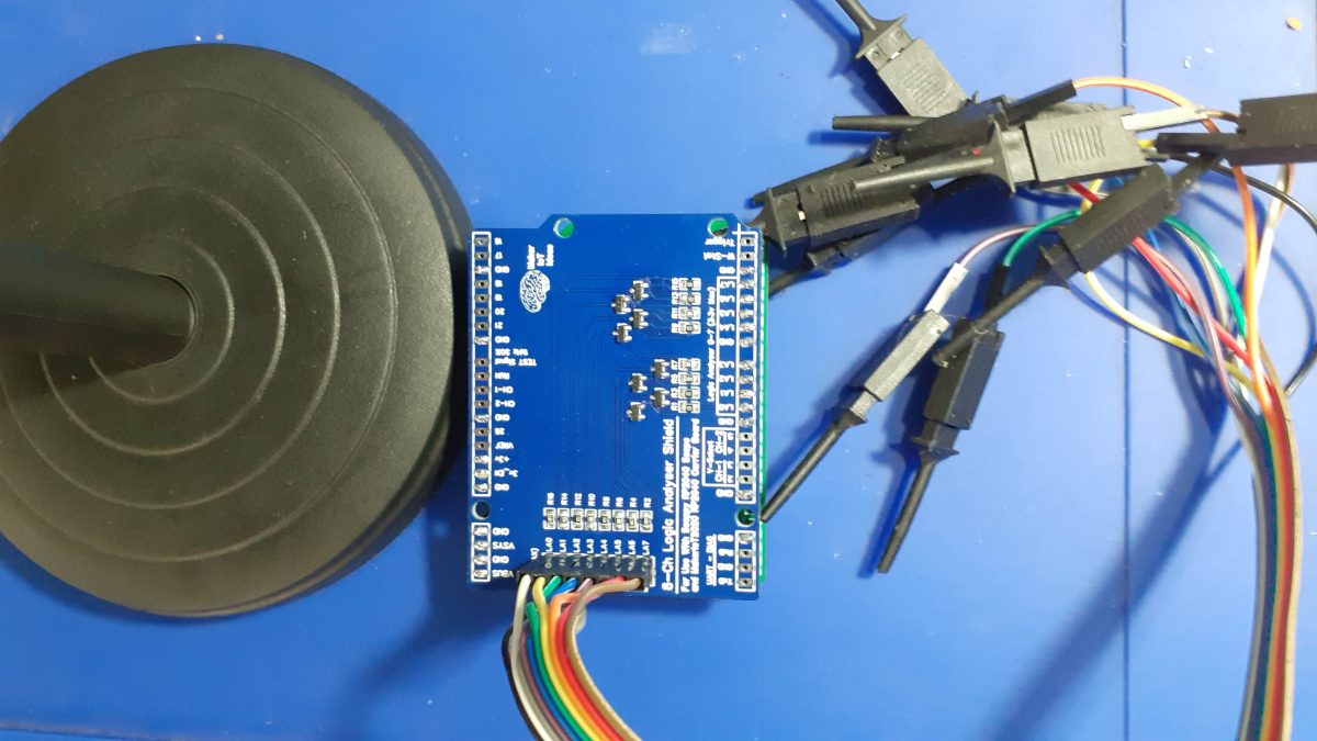
8 Ch Logic analyser Shield for use with Scoppy and MakerIOT2020 Pico Carrier Board
All Raspberry Pi Pico pins are broken out and labelled, as well as all of the pins specific to the Scoppy App have been clearly labelled. The board are stackable onto the Pico Carrier board, via standard 2.54mm Male Headers, or extra long, stackable female 2.45mm headers, similar to those found on common Arduino shields.
The use of stackable headers will allow simultaneous use of the logic analyser shield and the Analog frontend shield, introduced in part 3 of this series.
In addition to that, a 2×8-way 2.54mm Male header provides access to the 8 logic converted logic analyser inputs.
Logic conversion is done with a simple circuit, comprising a Bss138 N-Channel Mosfet and two 10K resistors per channel.
The shield is powered directly from the Pico Carrier board, which is in turn powered from the OTG cable to the Android Phone or tablet used to display the captured data. ( see Part 1 for installation instructions and other details regarding the Scoppy Project)
The logic level converters allow the use of a 5v logic signal, which is an improvement over the original design, which allowed only 3.3v inputs.
The PCB for this project has been manufactured at PCBWay. Please consider supporting them if you would like your own copy of this PCB, or if you have any PCB of your own that you need to have manufactured.
Some more pictures of the device
FrontBackAssembled FrontAssembled BackLogic analyser shield together with RP2040 carrier boardStacked view 1Stacked view 2Stacked with logic probes
All credits for the development of the Scoppy firmware goes to fhdm-dev. This shield is a modification made by MakerIOT2020, and thus belongs to me. In the spirit of the original project, It will however be released to the public as a free open-source project ( free as in free download, free schematic, free design ). The PCB manufacturing files will be made available for free at a later stage, or can be ordered from PCBWay from this link
Oscilloscopes and Logic analysers are essential instruments for every serious electronics hobbyist. They are however quite expensive, and thus beyond the reach of many people starting out with electronics. Today, I will show you a cheap solution, an RP2040 Oscilloscope and Logic analyser…
Before we get started, we need to clear up a few things first: 1). This is not my own project. It was designed and built by someone else. 2). This is not a professional grade Oscilloscope or Logic analyser 3). The range of input voltages, as well as the frequencies that you can measure, are limited.
What is this, and why do I bother with it?
This post is about the Scoppy Occiloscope Firmware, designed by fhdm-dev. I have no affiliation with him/her, I came across this recently and found it useful in the sense that it may help others gain access to instrumentation to greatly help them with electronics.
I did design some derived pcb components that works with this project, in order to take care of some limitations that I saw in the original project. More on that in two follow-up posts, in which I will show you two PCB’s that I designed to use with this project, and analog Frontend ( based on a public design by fhdm-dev, as well as a Logic analyser shield, of my own design
before we do this, we need to look at the basic Scoppy design and its firmware.
Getting Started
You will need a few things to make use of this project, the most important will be the Scoppy App ( available from the Google Playstore ), and an Android Phone. You will also need a USB OTG Cable/hub for the phone, as well as a Raspberry Pi Pico or Pico W
I have decided to use my own Raspberry Pi Pico Carrier board for this project, as it will allow me to get away from the breadboard, as well as serve as a platform for easily expanding on the project via expansion shields, as you will see in later articles.
Makeriot2020 Raspberry Pi Pico Carrier Board
This PCB, in Arduino Uno form Factor, will make putting the entire project into a case quite easy, as well as hopefully keep the number of floating hookup wires to a minimum. ( hopefully reducing some notice and other stray signals from interfering too much with our signals)
After installing the application, which is quite easy, we need to load the firmware onto the RP2040. This is also extremely easy is you follow the guide at the top.
Please note that the Android app has two modes, a freeware mode, limited to one channel, and a paid version, with no limitations. I recommend that you consider buying the paid version, as it only costs a few dollars ( I paid $USD2), and will motivate the developer to keep working on the project, and improving it.
Scoppy Application, Main Interface – OscilloscopeScoppy MenuScoppy Logic Analyser Screen
As we can see, the interface is quite clean, and easy to use.
What are the limitations?
There are quite a few limitations, namely frequency and voltage input. From what I can understand, the frequency limit seems to be around 25Khz, with the voltage level limit being 0.0v to 3.3v ( as per the limit of the RP2040 ADC
Please make sure that you follow all instructions on the original page, as you can very easily damage your Android device as well as the Pico if you apply a voltage outside of the allowed range.
On the logic analyser side, It is also important to note that you should stay in the 0.0v to 3.3v range of the Pico GPIO’s.
While these limited ranges will definitely limit what you can do and measure, It will still be a very useful project. In the next part of this article, I will show you how I have solved the logic analyser voltage range issue… Allowing you to analyse 5v signals as well.
The Rp2040 chip from the RaspberryPi foundation should be quite well known to everybody by now. Many companies have also released their own development boards based on it. The original Raspberry Pi Pico is popular, based on its small size.
For myself, there is however a serious drawback, its small size, while perfect for breadboard, made it necessary for the developers to place the pinouts on the back of the board. This makes it necessary to either memorise the pinouts or always have a pinout diagram handy when working with it.
The module also comes with castellated holes, making it ideal to place onto a custom PCB as a “component”. This got me thinking, I can easily design a custom RP2040-based PCB, but manually assembling the tiny RP2040 is something that my poor eyesight will make a bit challenging (staring at computer screens for many years does really take its toll as you get older).
Finding components in stock (excluding the RP2040) is also a challenge in my area.
This made me think about taking a popular footprint ( like the Arduino Uno ), and placing a Pico module directly onto the board, labelling all the pins clearly on the front, and installing female headers to access them.
While it is obviously not a very complicated PCB, it will definitely help me to utilise the fantastic little chip more effectively.
Assembling the PCB should only take a few minutes, as you only have to solder the pico and female header pins to the board. When completed, it should look like this:
If you have already soldered headers to your Pico, you can still use this PCB as well. You can also use the new Pico W with this board, the only difference is that the Pico W does not have castellated holes on the pins, so you would have to use header-pins. Also, the debug port now has a connector, so you will have to use the port directly on the Pico for that.
A good introduction to the new Pico-W can be found here. I have not bought any yet, so have no pictures to show, or comments to make on its operation.
What is next
I have plans to start designing a series of add-on shields with specific functions for this platform, since being freed from the breadboard, the Raspberry Pi Pico suddenly became much more interesting to me.
While smaller seems to be better in the electronics world of today, breadboarding, in my humble opinion, is quite aged, and can be extremely unreliable, due to poor connections etc. It is however very quick and fast, without requiring you to solder anything.
I am thus attempting to get the best of both worlds, by not being tied down to a breadboard, but with the freedom to go there if I choose, or just designing and using a custom shield of my choosing.
Manufacturing
Over the past eight years, PCBWay has continuously upgraded their MANUFACTURING plants and equipment to meet higher quality requirements, and now THEY also provide OEM services to build your products from ideas to mass production and access to the market.
The PCB for this project has been manufactured at PCBWay. Please consider supporting them if you would like your own copy of this PCB, or if you have any PCB of your own that you need to have manufactured.
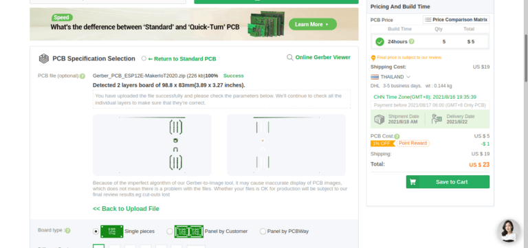
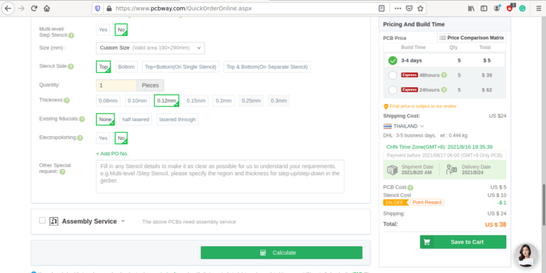
If you would like to have PCBWAY manufacture one of your own, designs, or even this particular PCB, you need to do the following… 1) Click on this link 2) Create an account if you have not already got one of your own. If you use the link above, you will also instantly receive a $5 USD coupon, which you can use on your first or any other order later. (Disclaimer: I will earn a small referral fee from PCBWay. This referral fee will not affect the cost of your order, nor will you pay any part thereof.) 3) Once you have gone to their website, and created an account, or login with your existing account,
4) Click on PCB Instant Quote
5) If you do not have any very special requirements for your PCB, click on Quick-order PCB
6) Click on Add Gerber File, and select your Gerber file(s) from your computer. Most of your PCB details will now be automatically selected, leaving you to only select the solder mask and silk-screen colour, as well as to remove the order number or not. You can of course fine-tune everything exactly as you want as well.
7) You can also select whether you want an SMD stencil, or have the board assembled after manufacturing. Please note that the assembly service, as well as the cost of your components, ARE NOT included in the initial quoted price. ( The quote will update depending on what options you select ).
8) When you are happy with the options that you have selected, you can click on the Save to Cart Button. From here on, you can go to the top of the screen, click on Cart, make any payment(s) or use any coupons that you have in your account.
Then just sit back and wait for your new PCB to be delivered to your door via the shipping company that you have selected during checkout.
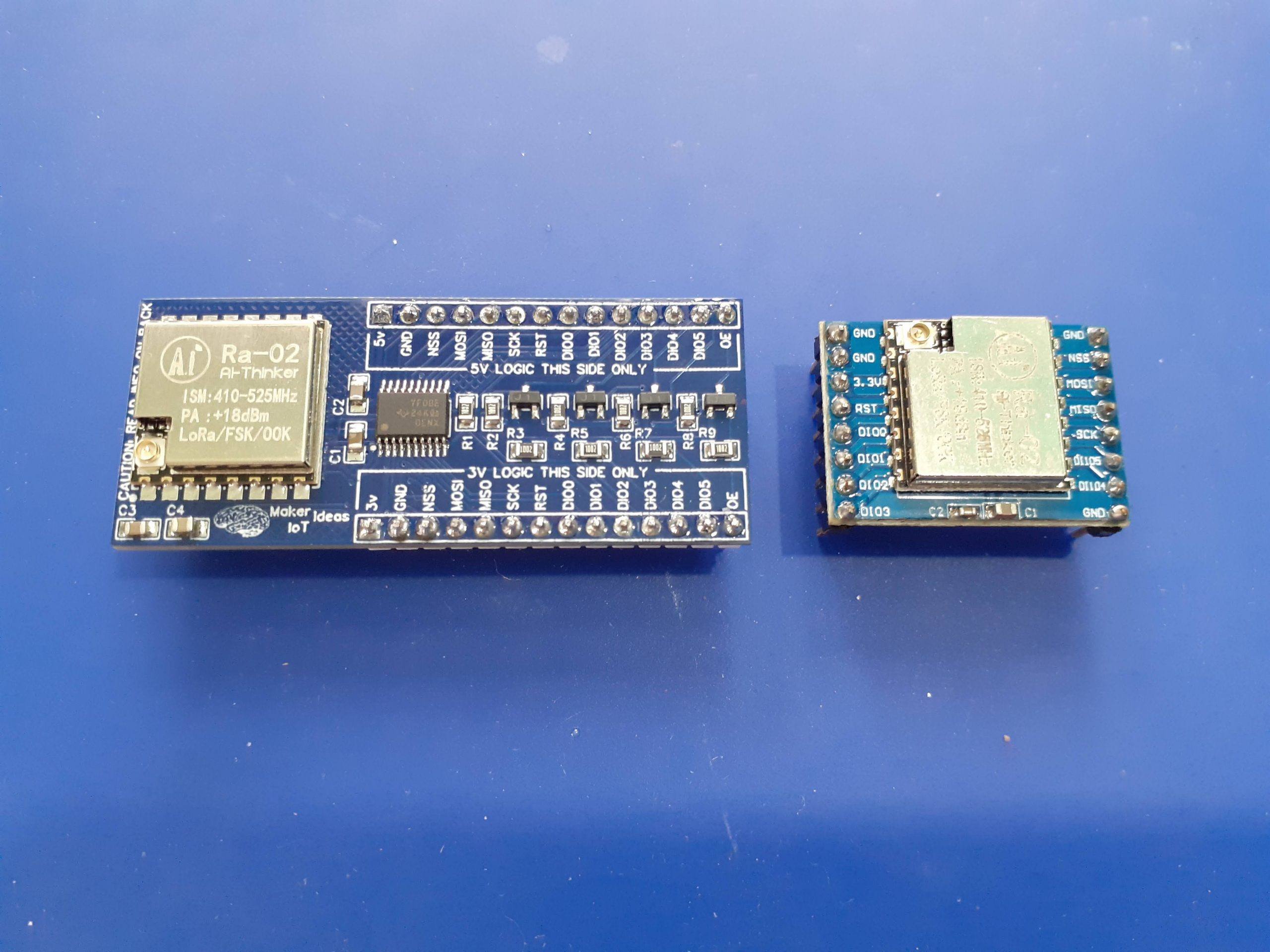
Most Makers and electronics enthusiasts may already know of the RA-02 LoRa Module. Many of them might own an RA-02 Breakout module or two… For those who do, they will surely know about the problems encountered with using this particular breakout module…
The RA-02 module, in itself, is a great piece of kit, and when used on a custom PCB, which was designed with all the little secrets of this module taken into consideration, is a pleasure. Using the RA-02 breakout module, in its existing form factor, does however present quite a few unique challenges, which, if you are unaware of them, can cause quite a few frustrating moments, or even result in permanent damage to the module…
1) The module is based on the SX1278 chip from Semtech and is a 3v device. The IO pins are NOT 5v compatible but seem to work for a few hours or so when used with 5v… This causes many people, especially on Youtube, to assume that it is ok to send 5v logic signals to this module…
I have still not seen any Youtube video telling viewers to at least use a resister divider or logic converter… People just don’t know, and those that know seem to be keeping quiet!
Adding logic converters is in fact specified by the datasheet.
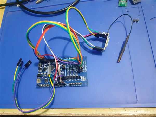
2) Adding logic converters means adding additional wiring, and for a breadboard based project, that adds to the complexity.
3) You have a total of 4 ground pins that need to be connected. not connecting all of them, causes funny things to happen, from overheating down to failure… ( My personal experience while researching this project)
4) The existing breakout module is not breadboarding compatible, resulting in a floating assembly with wires going everywhere, which results in unstable connections etc…
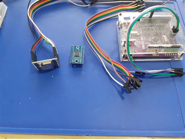
Basically something similar to the picture below:
In this picture, I have an existing RA-02 Breakout Module, with an 8 channel Logic converter and an Arduino Uno clone, along with all the needed wiring to make this setup possible… Quite a lot of wires indeed…
My solution:
I design and use quite a few LoRa PCBs and on all of them, I implement logic conversion using the BSS138 N-MOS Mosfet and 10k resistors. It is a cheap and reliable solution, but it can take up quite a lot of space on a PCB, as this means 11 Mosfets and 22 10k resistors if I were to provide level conversion to all of the RA-02’s GPIO and IO pins…
I also have the constant problem of many unnecessary wires, many of which sometimes fail straight out of the box, when prototyping something. I partly solved that by designing a few dedicated PCB solutions, but that is not always ideal,
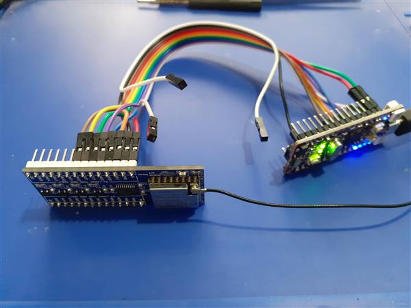
Using a dedicated Logic Converter IC, and Mosfet based converters to make up the difference, on a breadboard compatible module, seemed like a good idea, so I went ahead and designed the following solution:
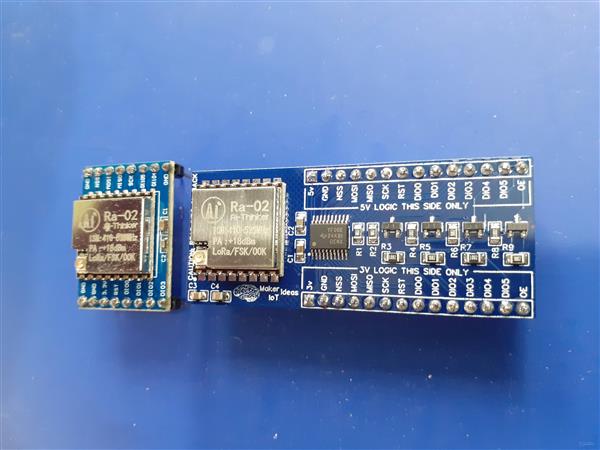
The breakout board module is breadboard compatible, and also has clearly marked pins to indicate the 3v and 5v sides of the module.
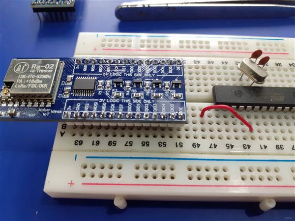
For my first test, I decided to test with an Arduino Uno Clone, since that is what most Makers and students will have access to. I used Cytron’s Maker Uno platform, which is equipped with some added goodies, in the form of diagnostic LED etc to make prototyping a lot easier.
As we can clearly see, It is only necessary to connect to the 5v logic side of the module, as well as provide 3v and 5v + GND to the module
In this test, I used Sandeep Mistry’s LoRa Library, with the Arduino IDE to do a quick test sketch.
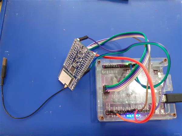
As we can see, you need quite a lot more wires to make this work. It is also worth noting that we have only 8 level converters on this ATMEGA328P PCB, in order to use all of the RA-02’s GPIO, we will need to add an additional external logic converter as well.
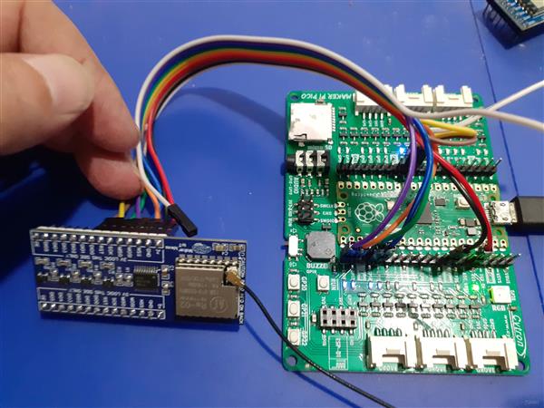
For my second test, I decided to be a bit brave, and try to use the new Raspberry Pi Pico ( RP2040 Microprocessor ). I have quite a few of them lying around and have never really done a lot with them, due to the fact that I do not really like using MicroPython or CircuitPython, and also because the recently released Arduino Core for the RP2040 still being quite new… I decided to use a development board that I recently bought from Cytron, the Maker Nano RP2040, as it has all the added diagnostic features to make my life a bit easier, I will also include a test with an original Pi Pico board, to make it more accessible to everyone out there.
Once again, I used Sandeep Mistry’s LoRa Library, with the exact same Arduino sketch, used for the Maker Uno test. (I obviously needed to change the pin numbers though, as the RP2040 uses different pins for its SPI interface).
Maker Nano RP2040 RA-02 Breakout Module
NSS 17
MOSI 19
MISO 16
SCK 18
RST 9
DIO0 8
In this case, we DO NOT need the OE pin, as the RP2040 is a native 3v device. The level converter can thus stay disabled, with its pins in tri-state ( high impedance ) mode.
If we look at the code, it is similar to the Maker Uno’s code, with only the Pin declarations needing a change
#include <SPI.h> // include libraries
#include <LoRa.h>
const int csPin = 17; // LoRa radio chip select
const int resetPin = 9; // LoRa radio reset
const int irqPin = 8; // change for your board; must be a hardware interrupt pin
byte msgCount = 0; // count of outgoing messages
int interval = 2000; // interval between sends
long lastSendTime = 0; // time of last packet send
// Note that SPI has different names on the RP2040, and it has 2 SPI ports. We used port 0
// CIPO (Miso) is on pin 16
// COPI (Mosi) is on pin 19
// SCK is on pin 18
// CE/SS is on pin 17, as already declared above
I did not use a breadboard, in order to make things as easy as possible.
To make things a bit easier, without having to resort to using a breadboard, I decided to do the Original Pi Pico test using the Maker Pi Pico PCB. This PCB is basically a big breakout module, with detailed pin numbers and some diagnostic LEDs, but it also uses a native Pi Pico, soldered directly to the PCB, by means of the castellated holes… So, While technically not being a true standalone Pico, It makes my life easier and was thus used for the test, as I can be sure that the pins are labelled exactly the same as on the original Pico.
The code used for the Maker Nano RP2040 works perfectly, with no changes required.
This post is getting quite long by now, so I have decided not to include my tests of the ESP-12E ( NodeMCU ) or ESP32 development boards here as well… They also function as expected.
In Summary
When I started this project, I set out to solve a problem ( personal to me ), that could potentially help a lot of other people use the RA-02 Module for more projects and tasks. The Breakout module in its current form can also be used with the RA-01h module (915Mhz Module) without any changes. All GPIO pins are broken out, and accessible through full logic converted pins on both sides of the breakout module.
I hope that this will be useful to someone. I am also not releasing the full schematics at this stage, as I may decide to make some minor cosmetic changes in the near future.
The PCB can however be ordered from PCBWay in its current form and works 100% as expected. The BOM file is available with the ordered PCB as usual.
This PCB was manufactured at PCBWAY. The Gerber files and BOM, as well as all the schematics, will soon be available as a shared project on their website. If you would like to have PCBWAY manufacture one of your own, designs, or even this particular PCB, you need to do the following… 1) Click on this link 2) Create an account if you have not already got one of your own. If you use the link above, you will also instantly receive a $5USD coupon, which you can use on your first or any other order later. (Disclaimer: I will earn a small referral fee from PCBWay. This referral fee will not affect the cost of your order, nor will you pay any part thereof.) 3) Once you have gone to their website, and created an account, or login with your existing account,
4) Click on PCB Instant Quote
5) If you do not have any very special requirements for your PCB, click on Quick-order PCB
6) Click on Add Gerber File, and select your Gerber file(s) from your computer. Most of your PCB details will now be automatically selected, leaving you to only select the solder mask and silk-screen colour, as well as to remove the order number or not. You can of course fine-tune everything exactly as you want as well.
7) You can also select whether you want an SMD stencil, or have the board assembled after manufacturing. Please note that the assembly service, as well as the cost of your components, ARE NOT included in the initial quoted price. ( The quote will update depending on what options you select ).
8) When you are happy with the options that you have selected, you can click on the Save to Cart Button. From here on, you can go to the top of the screen, click on Cart, make any payment(s) or use any coupons that you have in your account.
Then just sit back and wait for your new PCB to be delivered to your door via the shipping company that you have selected during checkout.
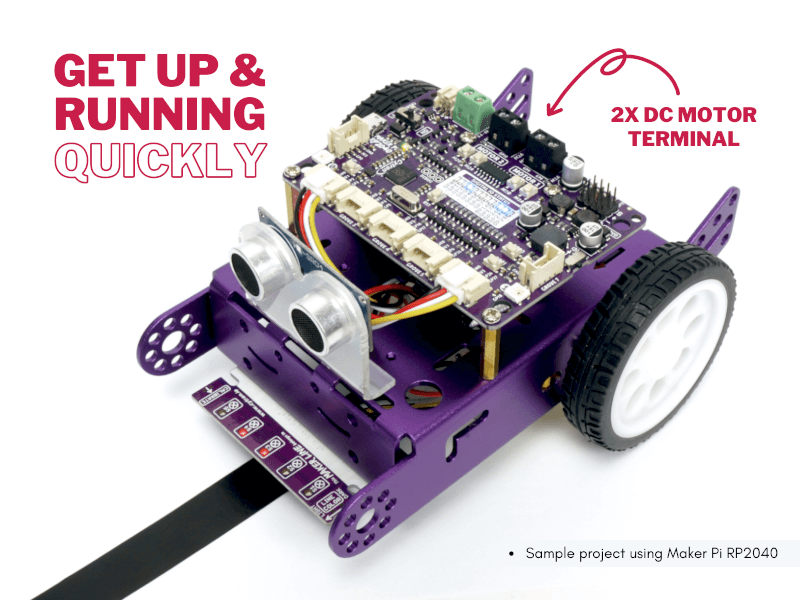
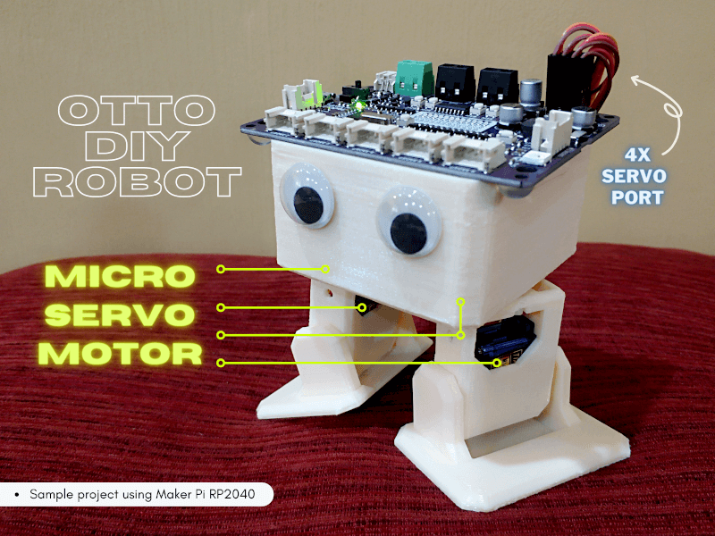
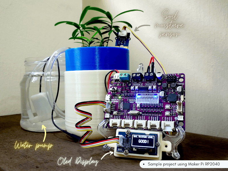
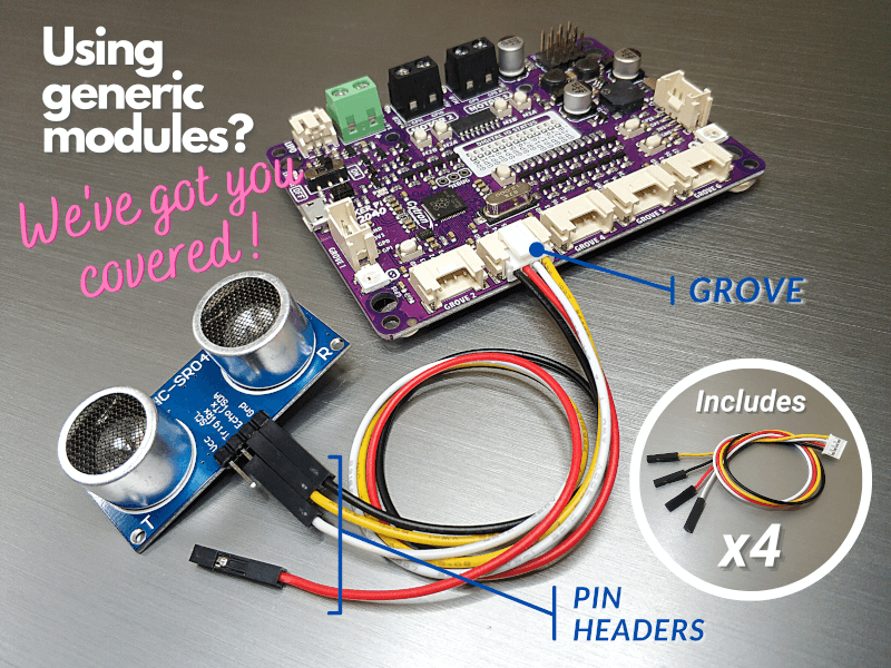
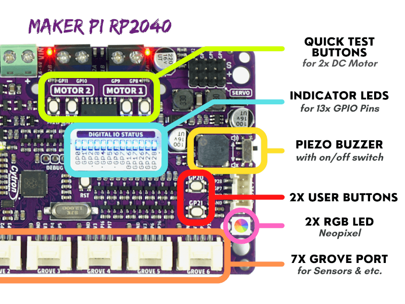
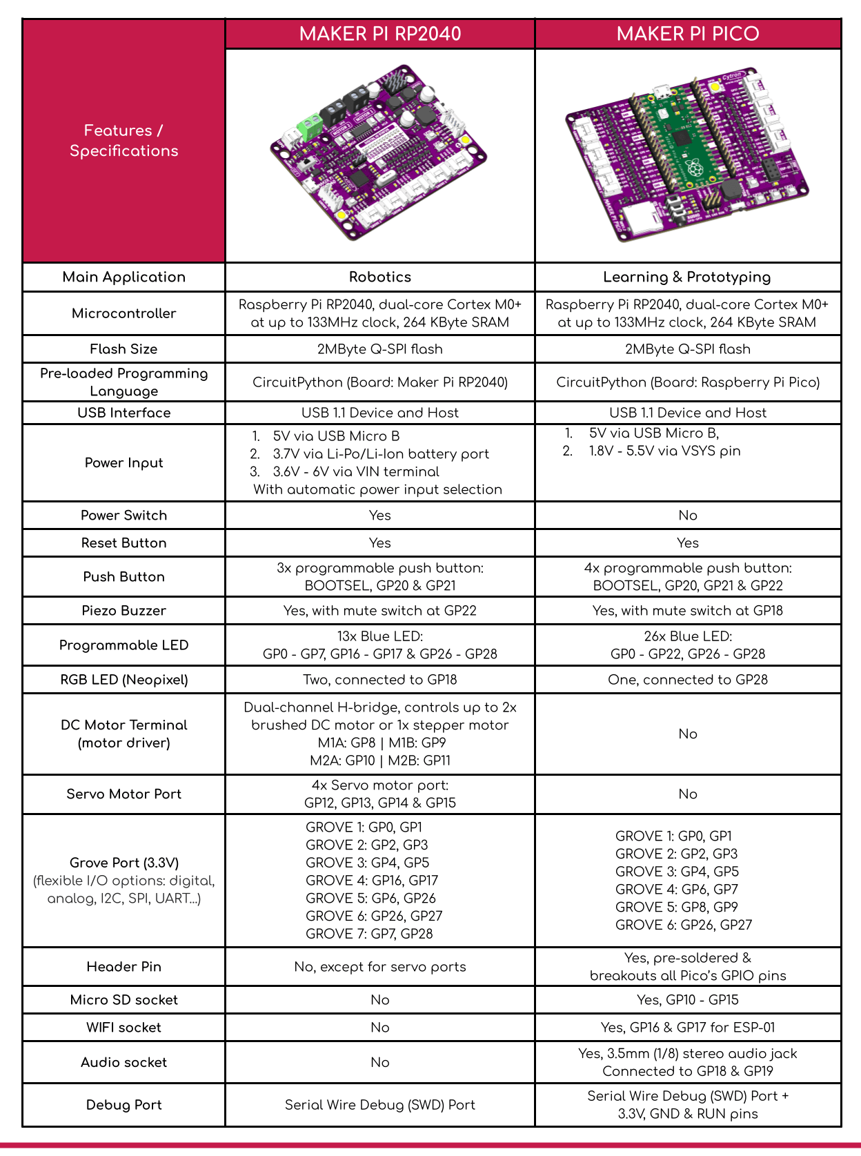
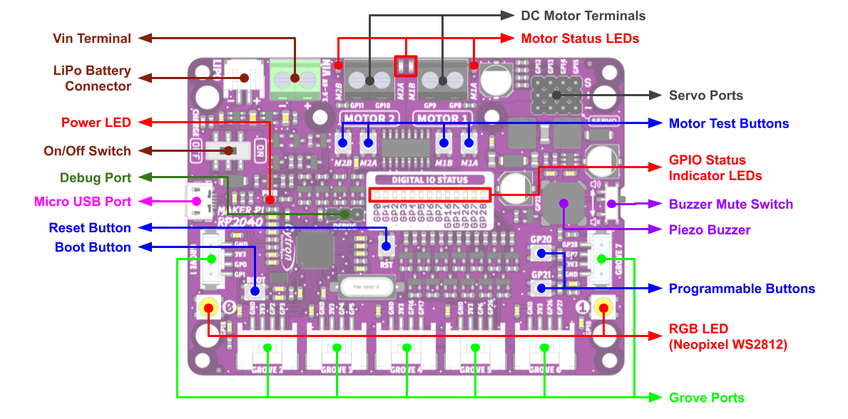
Cytron Maker Pi RP2040 features the first microcontroller designed by Raspberry Pi – RP2040, embedded on a robot controller board. This board comes with a dual-channel DC motor driver, 4 servo motor ports and 7 Grove I/O connectors, ready for your next DIY robot/motion control project. Now you can build a robot while trying out the new RP2040 chip.
The DC motor driver on board is able to control 2x brushed DC motors or 1x bipolar/unipolar stepper motor rated from 3.6V to 6V, providing up to 1A current per channel continuously. The built-in Quick Test buttons and motor output LEDs allow a functional test of the motor driver in a quick and convenient way, without the need of writing any code. Vmotor for both DC and servo motors depends on the input voltage supplied to the board.
Maker Pi RP2040 features all the goodness of Cytron’s Maker series products. It too has lots of LEDs useful for troubleshooting (& visual effects), is able to make quite some noise with the onboard piezo buzzer and comes with push buttons ready to detect your touch.
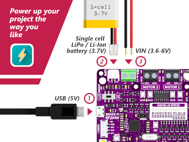
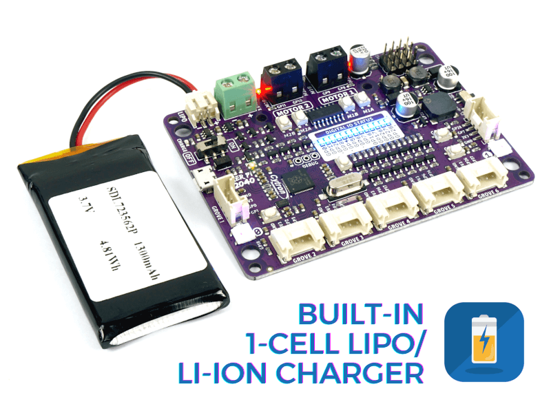
There are three ways to supply power to the Maker Pi RP2040 – via USB (5V) socket, with a single cell LiPo/Li-Ion battery or through the VIN (3.6-6V) terminals. However, only one power source is needed to power up both controller board and motors at a time. Power supply from all these power sources can all be controlled with the power on/off switch onboard.
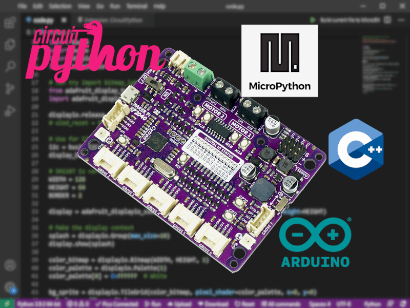
Cytron Maker Pi RP2040 is basically the Raspberry Pi Pico + Maker series’ goodness + Robot controller & other useful features. Therefore this board is compatible with the existing Pico ecosystem. Software, firmware, libraries and resources that are developed for Pico should work seamlessly with Cytron Maker Pi RP2040 too.
CircuitPython is preloaded on the Maker Pi RP2040 and it runs a simple demo program right out of the box. Connect it to your computer via USB micro cable and turn it on, you will be greeted by a melody tune and LEDs running light. Press GP20 and GP21 push buttons to toggle the LEDs on/off while controlling any DC and servo motors connected to it to move and stop. With this demo code, you get to test the board the moment you receive it!
While connected to your computer, a new CIRCUITPY drive appears. Explore and edit the demo code (code.py & lib folder) with any code editor you like, save any changes to the drive and you shall see it in action in no time. That’s why we embrace CircuitPython – it’s very easy to get started. Wish to use other programming languages? Sure, you are free to use MicroPython and C/C++ for Pico/RP2040. For those of you who love the Arduino ecosystem, please take a look at this official news by Arduino and also the unofficial Pico Arduino Core by Earle F. Philhower.
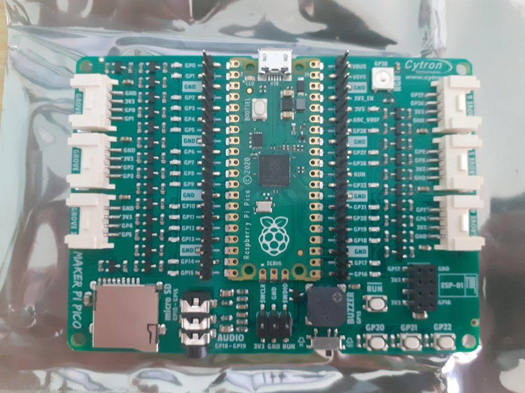
It has been almost a week now since I received my Maker Pi Pico from Cytron Technologies in Malysia. Most of this time has been spent getting to know the RP2040 Microchip, and how to effectively program it. Cytron has done an excellent job being very quick to market with a development board based on the RPi Pico, as well as providing a very good starting foundation to new Pico users ( which I believe is all of us, at least at this stage 🙂 )
It is super easy to put your Maker Pi Pico into Upload Mode. No need to plug and unplug your USB Cable. – Push and hold the RUN Button ( Located on the Bottom Right, Above the GP20 Push Button) . – While holding RUN pressed, press the BOOTSEL button on the Pico, and keep it pressed. – Release RUN and then release BOOTSEL.
You are now in BOOTSEL Mode. You can donload the official Micropython .uf2 file from the link below, or from the Raspberry Pi Website. It is also possible to install Micropython directly from inside the Thonny Python IDE.
It is not often that we get the opportunity to be one of the first people to get our hands onto a new product, So when my friends at Cytron Technologies asked me if I would like to do a review on a new Raspberry Pi product last week, I was definitely interested. Details were few, as the product was still under an NDA, but at last, I got the datasheets and some details on Tuesday, enough to start writing about the new product before the big Launch on Thursday the 21st of January 2021…
So, what am I trying to say? Well, It seems that the Raspberry Pi Foundation has released a new product, and from first impressions, it seems to be a game-changer… Lets not get confused. I am not speaking about a full size Raspberry Pi Board, or the compute module… No, The Pi Foundation has released an RP2040 Microprocessor based development board, in the same form factor as an Arduino Nano.
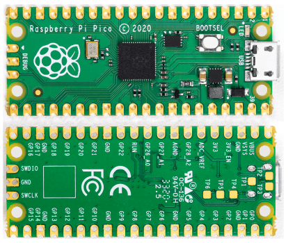
Raspberry Pi Pico Microcontroller Board
This will be an introduction post, and when I receive the device to play with, which will be soon, I will start with a short series on its features and capabilities… For now, lets look at some of the specifications
Front and Back view of the Raspberry Pi Pico
Features:
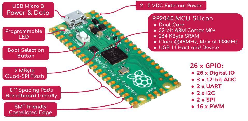
Raspberry Pi Pico has been designed to be a low cost yet flexible development platform for RP2040, with the following key features: • RP2040 microcontroller with 2MByte Flash • Micro-USB B port for power and data (and for reprogramming the Flash) • 40 pin 21×51 ‘DIP’ style 1mm thick PCB with 0.1″ through-hole pins also with edge castellations ◦ Exposes 26 multi-function 3.3V General Purpose I/O (GPIO) ◦ 23 GPIO are digital-only and 3 are ADC capable ◦ Can be surface mounted as a module • 3-pin ARM Serial Wire Debug (SWD) port • Simple yet highly flexible power supply architecture ◦ Various options for easily powering the unit from micro-USB, external supplies or batteries • High quality, low cost, high availability • Comprehensive SDK, software examples and documentation RP2040 key features: (Datasheet available for download at the bottom of this post) • Dual-core cortex M0+ at up to 133MHz ◦ On-chip PLL allows variable core frequency • 264K multi-bank high performance SRAM • External Quad-SPI Flash with eXecute In Place (XIP) • High performance full-crosspoint bus architecture • On-board USB1.1 (device or host) • 30 multi-function General Purpose IO (4 can be used for ADC) ◦ 1.8-3.3V IO Voltage (NOTE Pico IO voltage is fixed at 3.3V) • 12-bit 500ksps Analogue to Digital Converter (ADC) • Various digital peripherals ◦ 2x UART, 2x I2C, 2x SPI, up to 16 PWM channels ◦ 1x Timer with 4 alarms, 1x Real Time Counter • Dual Programmable IO (PIO) peripherals ◦ Flexible, user-programmable high-speed IO ◦ Can emulate interfaces such as SD Card and VGA
Pico provides minimal (yet flexible) external circuitry to support the RP2040 chip (Flash, crystal, power supplies and decoupling and USB connector). The majority of the RP2040 microcontroller pins are brought to the user IO pins on the left and right edge of the board. Four RP2040 IO are used for internal functions – driving an LED, on-board Switched Mode Power Supply (SMPS) power control and sensing the system voltages. Pico has been designed to use either soldered 0.1″ pin-headers (it is one 0.1″ pitch wider than a standard 40-pin DIP package) or can be used as a surface mountable ‘module’, as the user IO pins are also castellated. There are SMT pads underneath the USB connector and BOOTSEL button, which allow these signals to be accessed if used as a reflow-soldered SMT module.
The Pico uses an on-board buck-boost SMPS which is able to generate the required 3.3 volts (to power RP2040 and external circuitry) from a wide range of input voltages (~1.8 to 5.5V). This allows significant flexibility in powering the unit from various sources such as a single Lithium-Ion cell, or 3 AA cells in series. Battery chargers can also be very easily integrated with the Pico powerchain. Reprogramming the Pico Flash can be done using USB (simply drag and drop a file onto the Pico which appears as a mass storage device) or via the Serial Wire Debug (SWD) port. The SWD port can also be used to interactively debug code running on the RP2040.
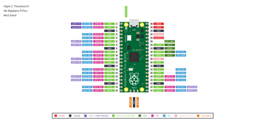
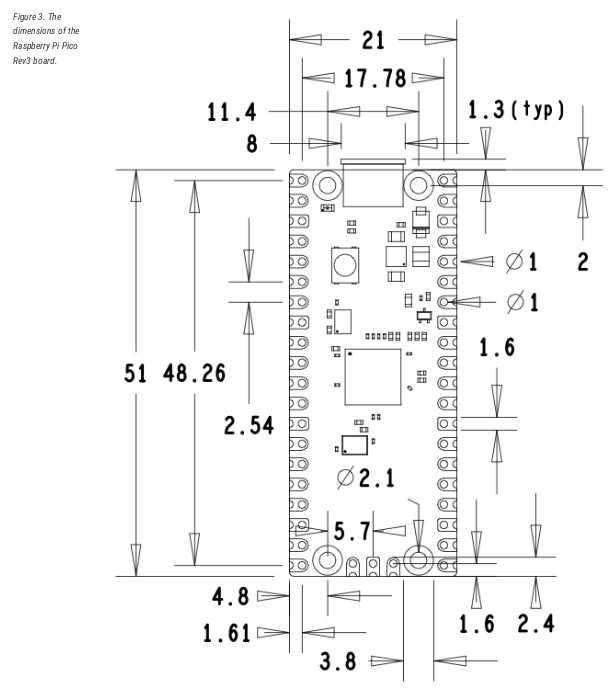
Mechanical Specifications
The Raspberry Pi Pico is a single sided 51x21mm 1mm thick PCB with a micro-USB port overhanging the top edge and dual castellated/through-hole pins around the remaining edges. Pico is designed to be usable as a surface mount module as well as being in Dual Inline Package (DIP) type format, with the 40 main user pins on a 2.54mm (0.1″) pitch grid with 1mm holes and hence compatible with veroboard and breadboard. Pico also has 4x 2.1mm (+/- 0.05mm) drilled mounting holes to provide for mechanical fixing, see Figure 3.
Mechanical specifications for the Raspberry Pi Pico
I hope that this is enough details to get all of you interested and eager for more details… In the next part of this series, I will focus on getting started with this new board, as well as do the official unboxing… Please stay tuned for more details…


