
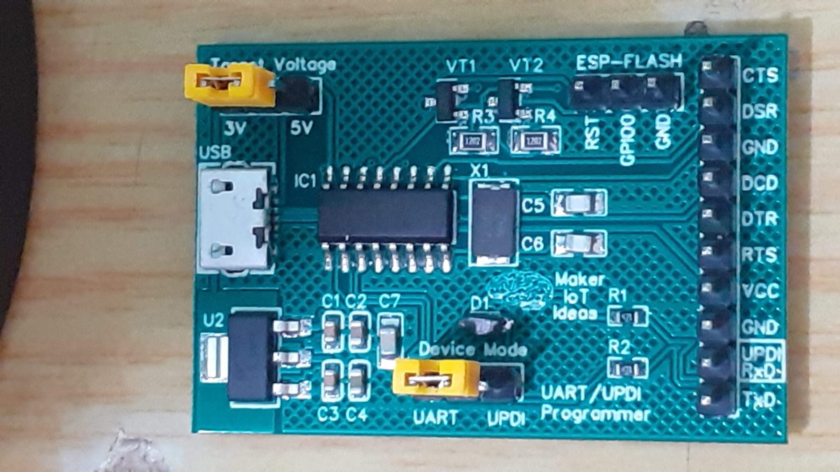
UPDI programmers are a new necessity in my lab, as I continue my quest to find a suitable replacement for the old Atmega328P chips (More on that in another post). In a previous post, I showed you a combination UART/UPDI programmer module that I have recently designed. It would only be fair to show you where that started out, as a single-purpose UPDI programmer, based on the CH340N.
The CH340N has, according to me at least, some advantages over the CH340G in the sense that it requires very few external components, most notably that it doesn’t require an external crystal oscillator. It does however NOT provide you with all the Modem signal lines (RTS, DTS, DTR, CTS etc) that you get on the CH340G, although most people will not use most of those anyway…
The cost of the two chips is about the same, with the CH340N being slightly more available at the moment, at least in my part of the world.
The particular circuit that I am using originated from Stefan Wagner. I simply designed my own PCB around his circuit. Credit is given where it is due, as I found his site, and content extremely detailed and accurate.
While this is a serial UPDI programmer, with NO HV capability, I do find it extremely useful as a test project, and while I may invest in a proper HV UPDI programmer in the future, if the bigger part of the project plays out the way I anticipate, for the time being, this is exactly what I need.
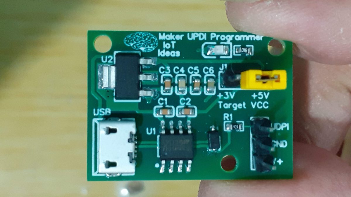
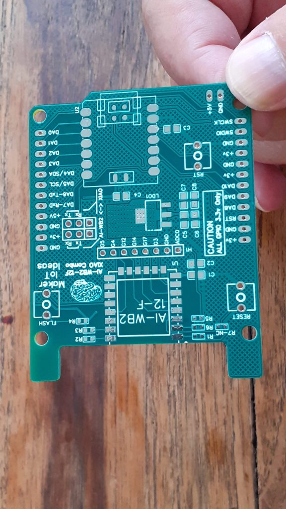
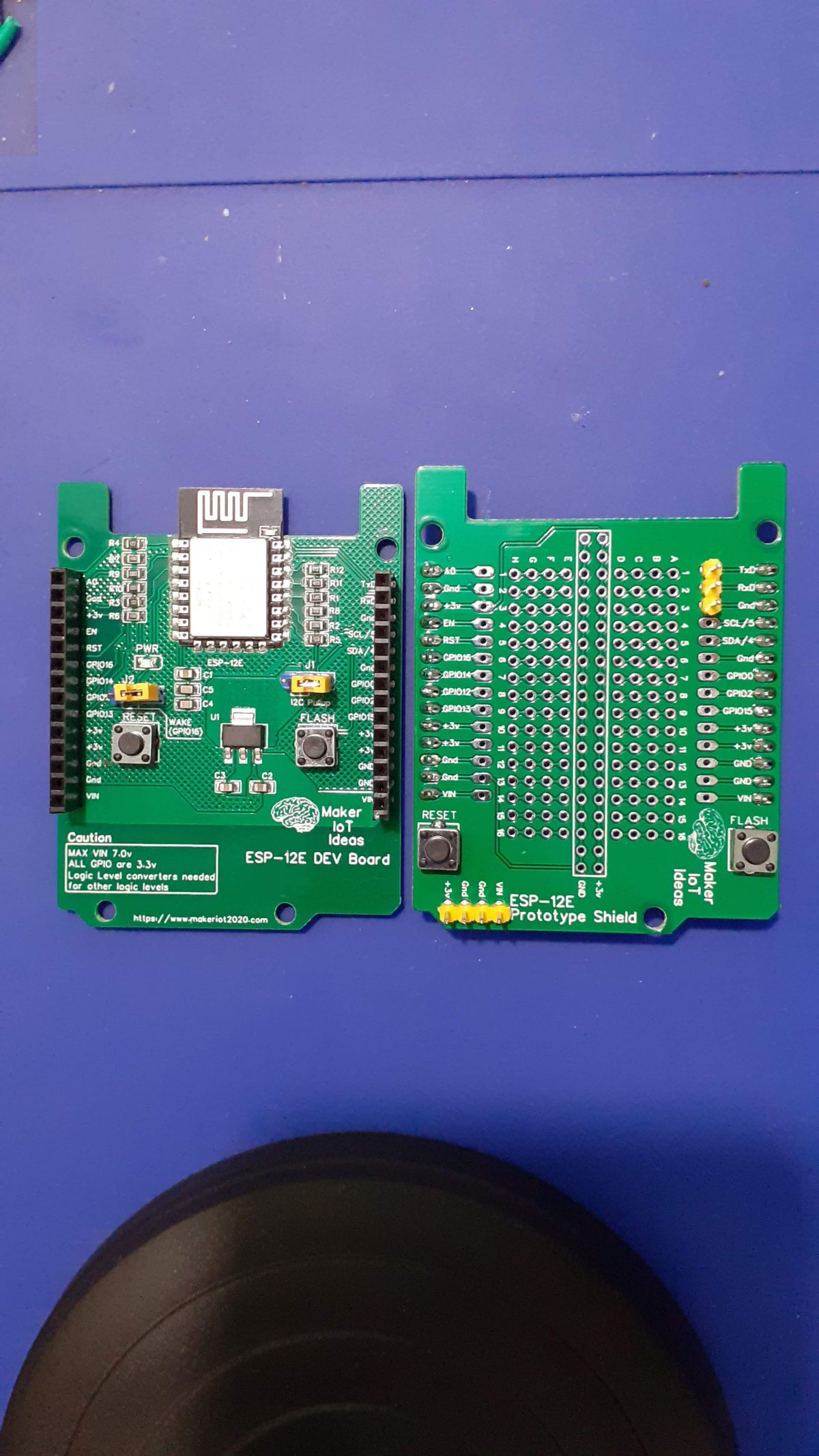
What is on the PCB?

The PCB is quite small, with a low component count, 6 capacitors, 4 of which is smoothing capacitors, two resistors, one Power on LED indicator, a 3.3v voltage regulator, USB connector ( Type B Mini) and of course the CH340N and a few header pins, one of which is used as a target voltage selector by means of a jumper. I did not bother with a switch as this pushes the cost of the device up by quite a bit.
Current costs for the components are around 5USD excl shipping at LCSC.
So, J1 is used to select the target voltage between 3.3v and 5v.
The other header provides VCC ( marked V+), GND and the UPDI output.
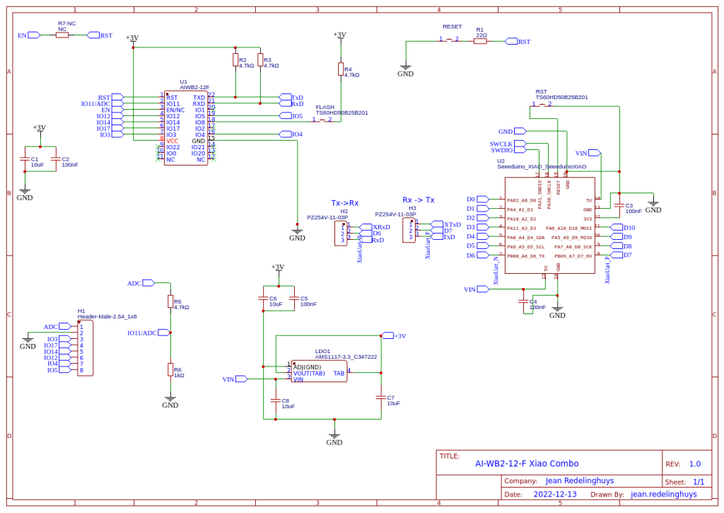
The Schematic

Manufacturing
As many of my existing readers will know by now, I choose PCBWay for my PCB manufacturing. Why? What makes them different from the rest?
PCBWay‘s business goal is to be the most professional PCB manufacturer for prototyping and low-volume production work in the world. With more than a decade in the business, they are committed to meeting the needs of their customers from different industries in terms of quality, delivery, cost-effectiveness and any other demanding requests. As one of the most experienced PCB manufacturers and SMT Assemblers in China, they pride themselves to be our (the Makers) best business partners, as well as good friends in every aspect of our PCB manufacturing needs. They strive to make our R&D work easy and hassle-free.
How do they do that?
PCBWay is NOT a broker. That means that they do all manufacturing and assembly themselves, cutting out all the middlemen, and saving us money.
PCBWay’s online quoting system gives a very detailed and accurate picture of all costs upfront, including components and assembly costs. This saves a lot of time and hassle.
PCBWay gives you one-on-one customer support, that answers you in 5 minutes ( from the Website chat ) , or by email within a few hours ( from your personal account manager). Issues are really resolved very quickly, not that there are many anyway, but, as we are all human, it is nice to know that when a gremlin rears its head, you have someone to talk to that will do his/her best to resolve your issue as soon as possible.
Find out more here

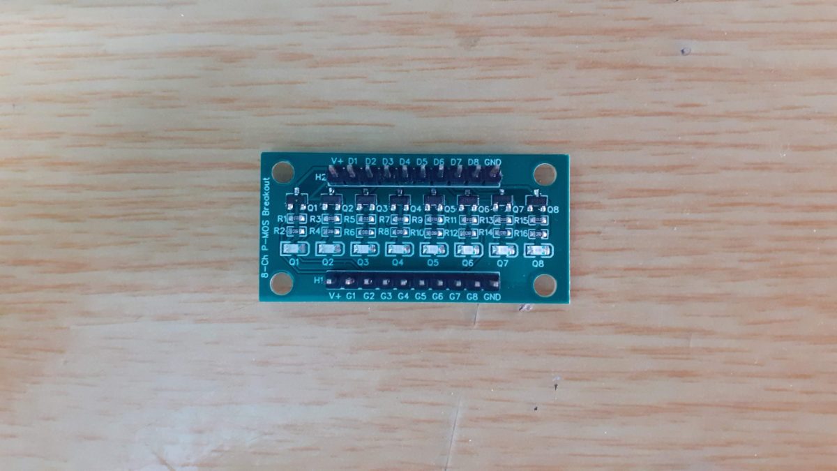
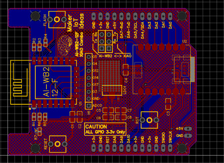
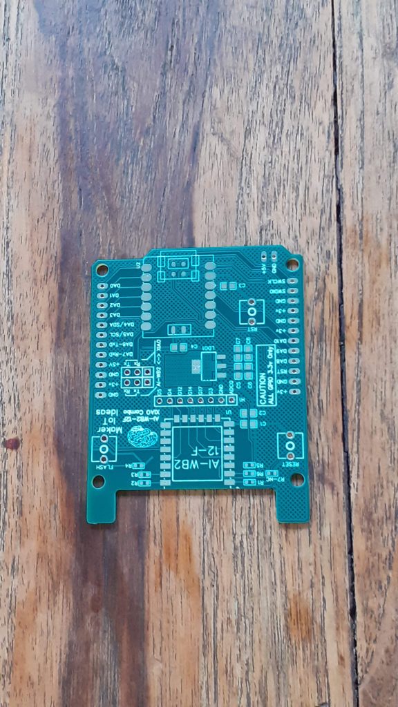
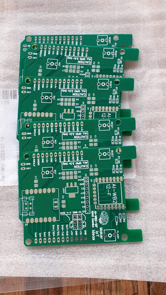
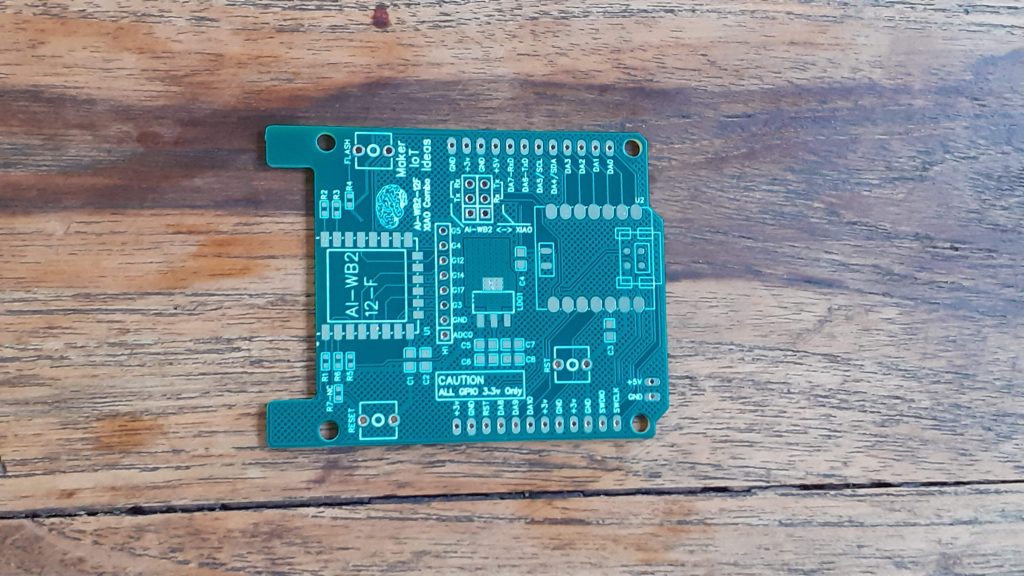
Pictures of the PCB and Assembled Module


Assembly
I assemble all of my projects by hand, using hot air and or a hotplate for reflowing. Having an accurate stencil for applying just the right amount of solder paste becomes a necessity very quickly.
In future, I plan to have a dedicated section showing the assembly of some of the more challenging boards…


