
Dc-to-DC Back converters have a lot of advantages over traditional linear voltage regulator solutions. Most of these advantages are related to the smaller size of these circuits, in comparison to their linear counterparts, as well as their higher efficiency and lower power consumption to name a few.
I am by no means a power supply guy, and as such, I usually buy my power supply modules. The same also applies to boost and buck converters. I am usually quite comfortable leaving the design of these critical parts to those who actually know what they are doing.
It thus seemed like a reasonable challenge to actually try and design and build one by myself, and that will be the story behind this post.

Finding a suitable driver IC
This journey started at a very strange place. When I decided to go ahead and build this Buck converter module, I had no specific driver IC in mind. I was thus browsing through the long list of dc-to-dc- buck converters on my component suppliers’ website, randomly pulling up a datasheet to take a closer look, mainly looking for something with as few external components as possible, while also having a decent current supply capability, as well as being able to operate on an input supply of 4v to about 24v, which is well within my usual range…
I eventually settled on the MPS MP9943. Definitely not the cheapest but still affordable, and in a QFN8 package, so that I am still able to actually solder it to a PCB!
-Wide 4V to 36V Continuous Operating Input
Range
-85mΩ/55mΩ Low RDS(ON) Internal Power
MOSFETs
-High-Efficiency Synchronous Mode Operation
-410kHz Switching Frequency
-Synchronizes from 200kHz to 2.2MHz
-External Clock
-High Duty Cycle for Automotive Cold-crank
-Internal Power-Save Mode
-Internal Soft-Start
-Power Good Indicator
-Over Current Protection and Hiccup
-Thermal Shutdown
-Output Adjustable from 0.8V
-Available in an QFN-8 (3mmx3mm)
package
and with a peak current supply of up to 3A – Not too bad at all.
The actual design
As mentioned already, I am not ( or at least I don’t see myself) a power supply design expert. I believe I am perfectly capable with the linear stuff, by switchmode was never my strong point 🙂 This prototype will just be based on the recommended design in the datasheet, at least for the first version, and then, later versions may feature some customisation as actually needed.

From the picture above, we can see that there are indeed not a lot of external components required. And in my humble opinion, the efficiency vs load also seems to be quite reasonable.
I thus went ahead and started reading this datasheet in detail. I found two typical-use circuits with recommended component values, from which I build my prototype.


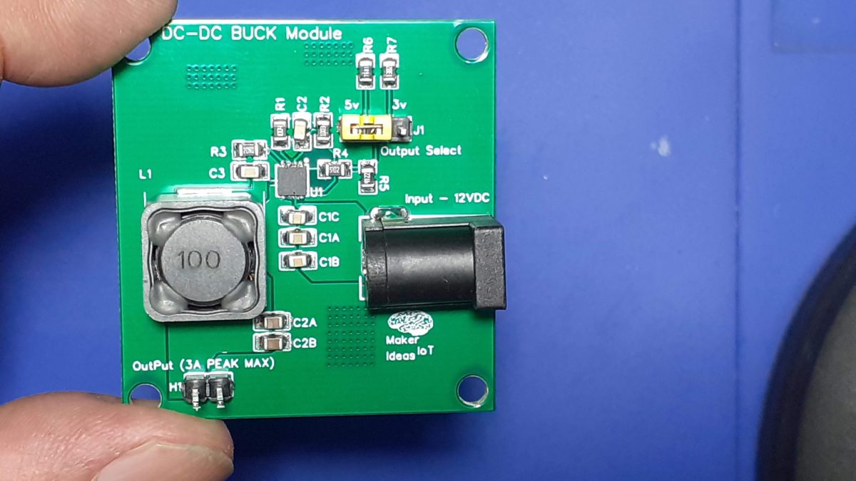
I chose to combine these two circuits to give me a variable output module, that will be selectable between 5v and 3v.
I also chose an inductor with a 6A maximum current rating, as the datasheet states that we should choose one with at least a 25% higher current rating than our peak requirement. My logic here was that 100% would be a good number, as the inductor would in theory never saturate?? as well as produce less heat etc ?? Please comment on this, as I may be barking up the wrong tree here 🙂

The schematic above is what I came up with. A jumper will allow the selection of the output voltage, as this is determined by the value of the resistor at R8, in my case 13K or 7.68k… I also assume that that resistor can later be replaced by a 20k trimpot or similar to give a truly variable output.
PCB Layout


The PCB layout was an attempt to follow the datasheet recommendations as closely as possible, while still having my own design. I am also aware that I may have wasted quite a bit of space, but for now, my focus is on getting a working design. I can always try to squeeze it into a smaller space later.
Manufacturing
I choose PCBWay for my PCB manufacturing. Why? What makes them different from the rest?
PCBWay‘s business goal is to be the most professional PCB manufacturer for prototyping and low-volume production work in the world. With more than a decade in the business, they are committed to meeting the needs of their customers from different industries in terms of quality, delivery, cost-effectiveness and any other demanding requests. As one of the most experienced PCB manufacturers and SMT Assemblers in China, they pride themselves to be our (the Makers) best business partners, as well as good friends in every aspect of our PCB manufacturing needs. They strive to make our R&D work easy and hassle-free.
How do they do that?
PCBWay is NOT a broker. That means that they do all manufacturing and assembly themselves, cutting out all the middlemen, and saving us money.
PCBWay’s online quoting system gives a very detailed and accurate picture of all costs upfront, including components and assembly costs. This saves a lot of time and hassle.
PCBWay gives you one-on-one customer support, that answers you in 5 minutes ( from the Website chat ), or by email within a few hours ( from your personal account manager). Issues are really resolved very quickly, not that there are many anyway, but, as we are all human, it is nice to know that when a gremlin rears its head, you have someone to talk to that will do his/her best to resolve your issue as soon as possible.
Find out more here

Assembly
After receiving the PCBs back from the factory, and receiving the components from the supplier, I started on the assembly. While uneventful, It was worth mentioning that this project does require a stencil. The DFN-8 package is quite small (only 3mmx3mm), with eight leads, so that makes for some tiny spacing between them. As it is also a leadless package, I did not want to chance to have too much solder paste in there.

As we can clearly see in the picture above, the pads are super tiny. The other components are 0805 ( for reference).
My standard way for assembling DFN packages is to actually level the part of the PCB while reflowing the PCB with a hotplate. Then, when the solder has all melted and is in a liquid state, I carefully place the part with tweezers and remove the PCB from the hotplate.
Alternatively, I remove the PCB from the hotplate first, leaving it to cool down a bit, and then, using a hot air gun with a small nozzle, reflowing only the area where the part needs to be placed, and carefully placing it onto the melted solder.
Both of these methods seem to be working quite well, for me at least, but the hot air method does however have the risk of a bit of solder splatter, which may form unwanted bridges… The part also gets heated a bit, as it has to be held in place for a few seconds to prevent it from being blown around by the hot air.
Testing

I am quite happy to report that the module works as expected, with a steady output of 3.31v and 5.08v respectively at no load.
Under load, I tested with a 1A and 2A load respectively, both voltages are also stable. Ripple, as measured by myself, and using a “not too good” digital oscilloscope, seems to be about 110mv peak-to-peak.
Using better probes, and a better scope, I may be able to get a better and more accurate reading.
Conclusion
This was quite an exciting project, with setting myself a challenge, and actually achieving what I set out to do. While I am sure that the module in its current state may actually not quite be perfect, and that it surely has a lot of room for improvement, I am satisfied with its performance, and just plainly, the fact that it actually works!


