
A few weeks ago, I started looking into alternative development solutions to reduce the effect of hard-to-get or more expensive-than-usual ATMEGA328 chips. One of the chips that I found to have potential was the ATTiny1616.
There seemed to be quite a lot of stock, and the prices were reasonable. Some additional hardware, like a dedicated UPDI programmer, had to be designed or bought, as the ATTiny1616 required UPDI to upload and flash code.

While the breakout worked flawlessly, I found the programming setup awkward and cumbersome. That was the cue to take the next step and create something that was easier to work with.

The new PCB offers a development cycle that is very similar to a standard Arduino UNO or Nano. Plug it into a USB port, write code, upload and repeat…
What is on the PCB?

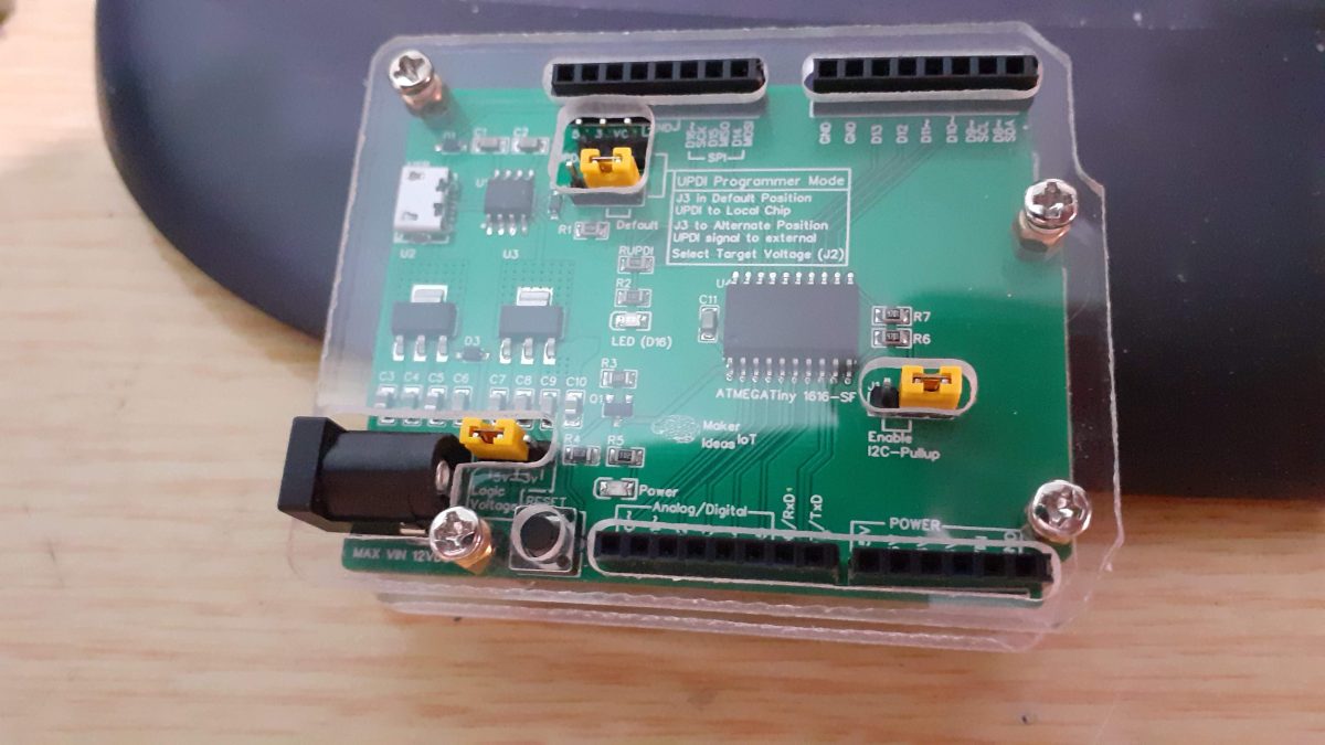
Starting at the Top Lefthand corner, we have a USB port, with a CH340N Chip. Note that this IS NOT A SERIAL UART. This is an integrated UPDI programmer, that can also be used in stand-alone mode to program external devices. (by moving J3 to the left, and using the UPDI header).
Below that is the power supply section, featuring two LDO Voltage regulators, providing 3.3v and 5v DC to the system. A DC barrel jack is included, to supply between 7v and 12v external DC voltage to the system. ( NOT to be used together with a USB cable)
Jumper J2 (next to the DC barrel jack) is used to switch the entire board logic level between 3.3v and 5v DC. A power indicator LED, as well as a standard user LED ( on pin D16), is also included. The rest of the PCB is dedicated to the ATTiny 1616 -SF, this time in a TSOP form factor. ( The original breakout used a QFN, but I realised that that may push away a lot of potential users, as QFN packages are quite difficult to solder without the proper equipment. A TSOP package is more accessible to everyone)

A total of 17 GPIO ports are available, of which each is labelled with an Arduino compatible label (D0 – D15), PWM ~ capable pins, and alternate functions like UART, SPI and I2C. Please Note that the onboard USB port IS NOT A UART
Features on the PCB – Summary
- Reset Circuit with Push button – The ATTiny1616 shares its Reset pin with the UPDI programming pin. This will cause problems, requiring an HV UPDI programmer to fix. To resolve this issue, a reset circuit, comprising of a p-channel logic level Mosfet, that is wired to be constantly on, is connected via a suitable resistor on its gate, to a push-button to ground. pressing the button pulls the gate to ground, switching off the Mosfet, and thus the supply voltage to the chip, which equates to a power cycle reset. It is worth noting that the UPDI programming sequence also auto-resets the chip after every upload.
- DC barrel jack for powering the device from an external source – 7v to 12DC
- Onboard I2C pull-up resistors, selectable with a jumper ( J1)
- Onboard UPDI programmer, which can also be used in stand-alone mode.
- Selectable voltage logic level between 3.3v and 5.0v ( J2)
Manufacturing
I choose PCBWay for my PCB manufacturing. Why? What makes them different from the rest?
PCBWay‘s business goal is to be the most professional PCB manufacturer for prototyping and low-volume production work in the world. With more than a decade in the business, they are committed to meeting the needs of their customers from different industries in terms of quality, delivery, cost-effectiveness and any other demanding requests. As one of the most experienced PCB manufacturers and SMT Assemblers in China, they pride themselves to be our (the Makers) best business partners, as well as good friends in every aspect of our PCB manufacturing needs. They strive to make our R&D work easy and hassle-free.
How do they do that?
PCBWay is NOT a broker. That means that they do all manufacturing and assembly themselves, cutting out all the middlemen, and saving us money.
PCBWay’s online quoting system gives a very detailed and accurate picture of all costs upfront, including components and assembly costs. This saves a lot of time and hassle.
PCBWay gives you one-on-one customer support, that answers you in 5 minutes ( from the Website chat ), or by email within a few hours ( from your personal account manager). Issues are really resolved very quickly, not that there are many anyway, but, as we are all human, it is nice to know that when a gremlin rears its head, you have someone to talk to that will do his/her best to resolve your issue as soon as possible.
Find out more here

Assembly

While this board can definitely be assembled completely by hand soldering, I chose to make use of a stencil, from PCBWay. This helps me by ensuring that the solder paste is applied in exactly the correct amount and place. Hot air or reflow soldering afterwards is a quick easy task. I prefer to use a hot plate to reflow the board, especially since it has a tiny USB connector, which can be quite a pain to solder with hot air, I won’t even go there with a normal soldering iron, as it is beyond what my eyes can handle at this stage.
Some more pictures


