
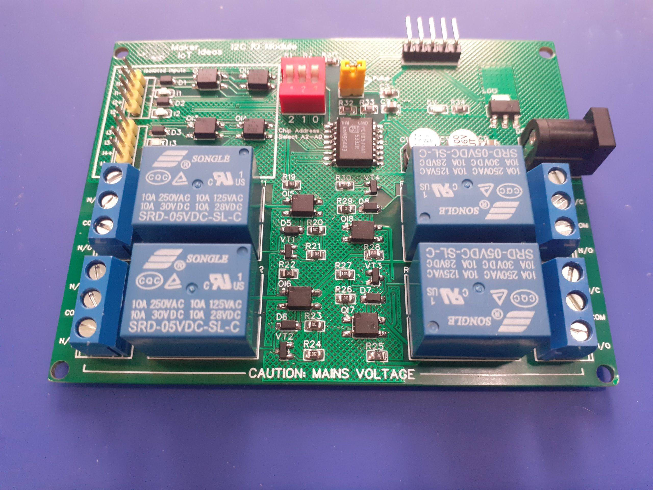
Sometimes we need extra Inputs or Outputs on a device, or for use with a project. To implement it properly we also need a lot of additional electronic components to properly isolate these inputs and outputs, with the signals they switch, from our own project, because, let us be real, electronics and electrical devices in the real world do not all work with Arduino or ESP32/ESP8266 save voltages ( 5v and 3.3v ).
I will also tell you about a very special deal to get PCBs of your own made for only one (1) USD ( Including shipping with DHL )! No, I am not joking, and I am not crazy either… More on that later in the post…
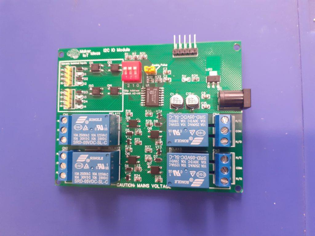
It is thus extremely important to have a module that can effectively interface with inputs of 5.5v up to 32v DC ( optically Isolated up to 3000v ), and relay outputs, also optically isolated at 3000v. ( Note that the optical isolation voltage does not mean you can input that voltage level into the chip! It means that it can isolate the electronics on the safe side of the isolator from a voltage spike of up to that voltage!).
I also love using I2C, as it allows me to add modules onto an existing data bus while using only 2 GPIO lines on the MCU!
The module I am presenting to you today was designed to be operated from 5v DC. That includes the I2C data lines (SDA and SCL). If you need to interface to a 3.3v microprocessor, like an ESP32 or ESP8266, or even the new RP2040 or an STM32, you need to use a logic level converter.
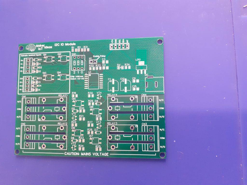

The PCB uses the popular PCF8574 8 channel IO expander, which is extremely easy to use, and where you can connect up to 8 devices in a chain ( 16 if you use the PCF8574AT variant as well.. Meaning eight of each variant) This surely adds up to quite a lot of IO lines at a cost of only 2 GPIO on your MCU!
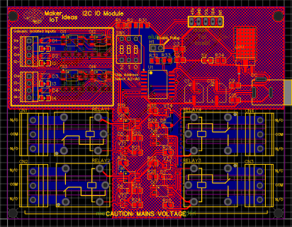
The Circuit diagram is below, and I will discuss each part briefly.
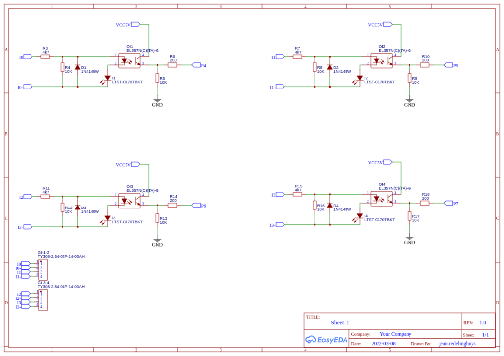
This is the Galvanic Isolated Input schematic. Each input operates at a voltage of 5.5v to 32v DC. Complete Galvanic Isolation between the Module and the remote input is in effect. Please note that you have to supply a remote ground from the device that provides the input. DO NOT connect the PCB Module ground to an isolated ground pin. This may still work but renders the galvanic Isolation for that input completely useless.
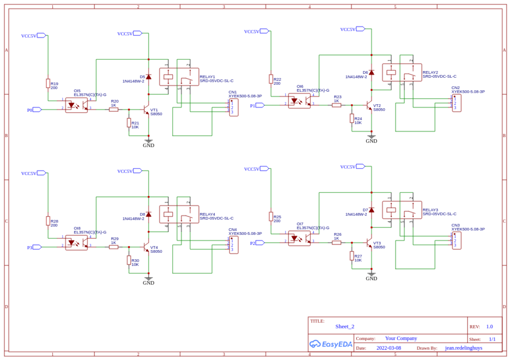
This is the Relay driver schematic. Each relay output is driven through an optocoupler, as well as a transistor. Although this arrangement does not provide complete galvanic Isolation of the relay coil, it does protect your MCU from any voltage spikes caused by back-emf when the relay is de-energised. The Relay contacts themselves, being magnetically actuated by the coil, are in themselves Galvanically Isolated from the rest of the PCB.
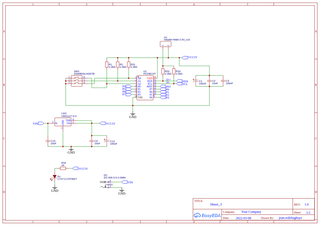
Finally, we have the I2C IO Expander schematic, with a 5v LDO regulator, capable of providing up to 600mA of current to the PCB. The PCF8574 Chip’s address is selectable with DipSwitch SW1 so that you can use multiple PCBs at the same time if you should choose to do so. The only note on that is that you should not connect the 5v lines of each individual PCB together. You should also only connect the GND and SDA, SCL lines back to the MCU.
Earlier on in the post, I promised to tell you about a very special deal…

Well, here it is, as well as some details about the sponsor of this very exciting deal…
PCBPartner.com is owned and operated by Kinji Group, which was established in 1997. We have over 20 years of experience in PCB manufacturing, PCB design, component manufacturing and distribution, PCB assembly and PCB cam software development.
While Kinji Group has 3 PCB factories in China, we have also developed strategic partnerships with more than 15 other factories around Asia. We, therefore, have a large group of specialists in PCB manufacturing, quality control, technical support and part sourcing to support your innovative ideas and products.
Our over 500 employees are spread across 8 branches in Mainland China (Shenzhen, Dongguan, Shanghai, Wuxi, Chengdu, Xiamen), Hong Kong SAR, and Taiwan. And we’re still growing!
We’re confident once you try us out, we’ll become your PCB Partner. And if not? Well, you’ll have scored some free PCB! So why not take us for a spin, you’ve got nothing to lose.
We, MakerIoT2020.com, have decided to give it a go and send this particular PCB to PCBPartner.com for manufacturing. So far, while we are still waiting to receive the PCB, ( Weekends happen 🙂 ), We are very happy with the ease of use of the online ordering system provided.
We would also like to point out that this special order will only be available until the end of March 2022,
as well as that there are a few conditions:
Promotion ends March 31st 2022
Each new customer can enjoy free PCB on their first order
This promotion applies to
1-2 layers of FR4 PCB, up to 100x100mm, 10pcs, with Green Solder Mask
4 layer of FR4 PCB, up to 50x50mm, 10pcs, with Green Solder Mask
1 layer Aluminum PCB, up to 100x100mm, 10pcs
This PCB promotion cannot be used with other discounts or other promotional activities
For a full list of conditions, and countries that may participate in this offer, please click on the link here
Let us have a look at the entire ordering process..
Once you click on the PCBPartner.com link, you will be taken to their website, where you should sign up, which is free and easy… We used our Google.com account details and were ready to order in seconds…
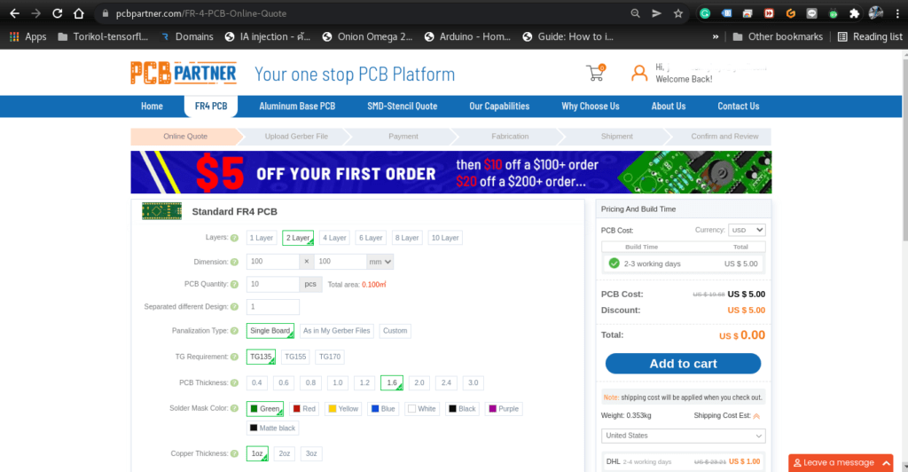
You can now Login with your new credentials ( after registering using this special link ). Then click on the FR4 button to start the order process…
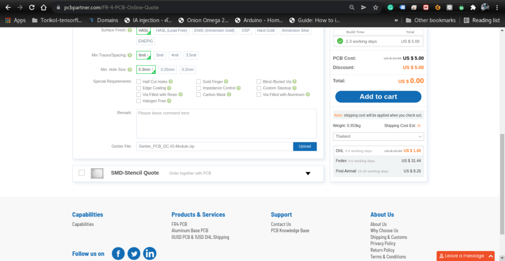
Enter the specific details for the manufacturing of your PCB, and upload your Gerber files.
Continue selecting options for your PCB order…
Make sure to select DHL shipping, to take advantage of the special 1USD option, and click on the ADD to Cart Button…
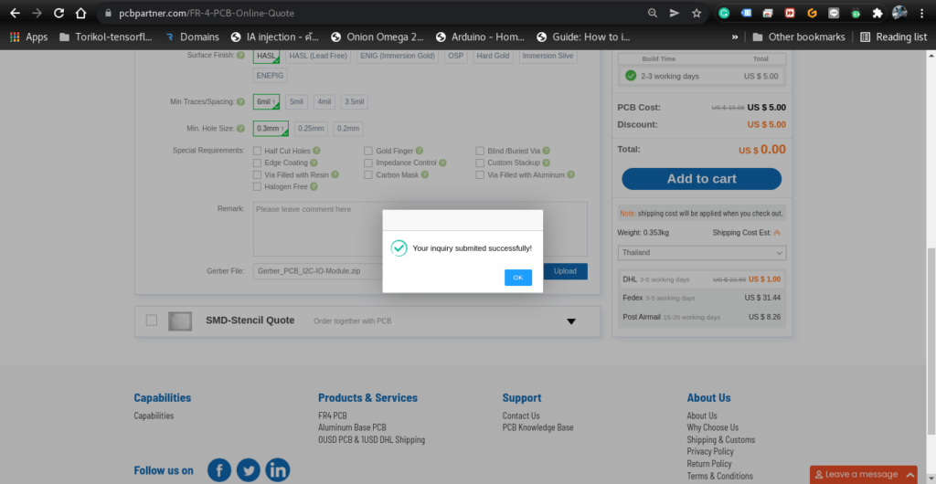
You will now get a message that your enquiry has been submitted successfully.
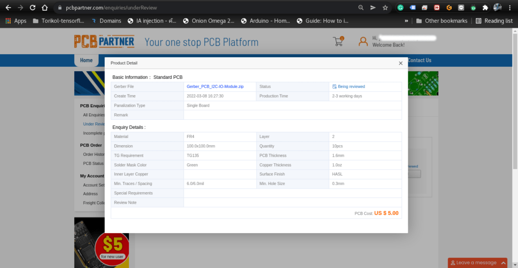
Click on the “Under review” button, to see your quote status… In my case, it took about 5 minutes for the review to pass, and be able to checkout and pay for the order…
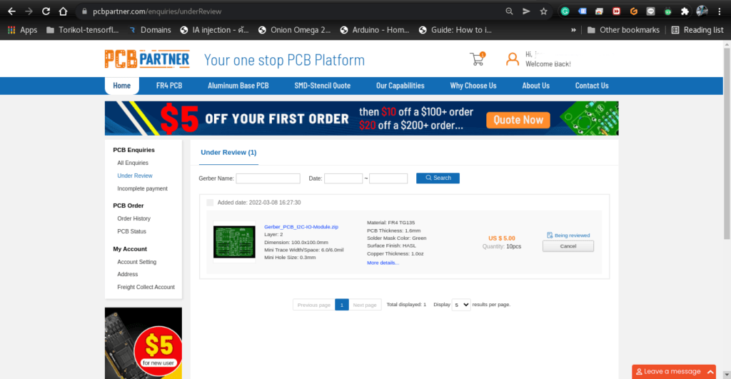
Once the review has passed, you will see a pending payment,
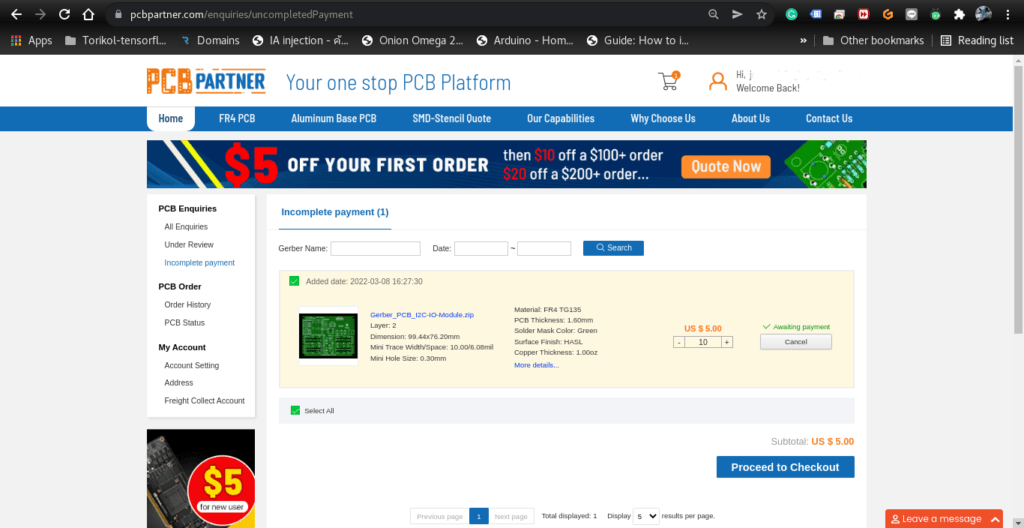
You may now click on the “Proceed to Payment” option
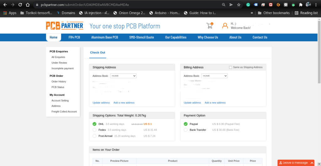
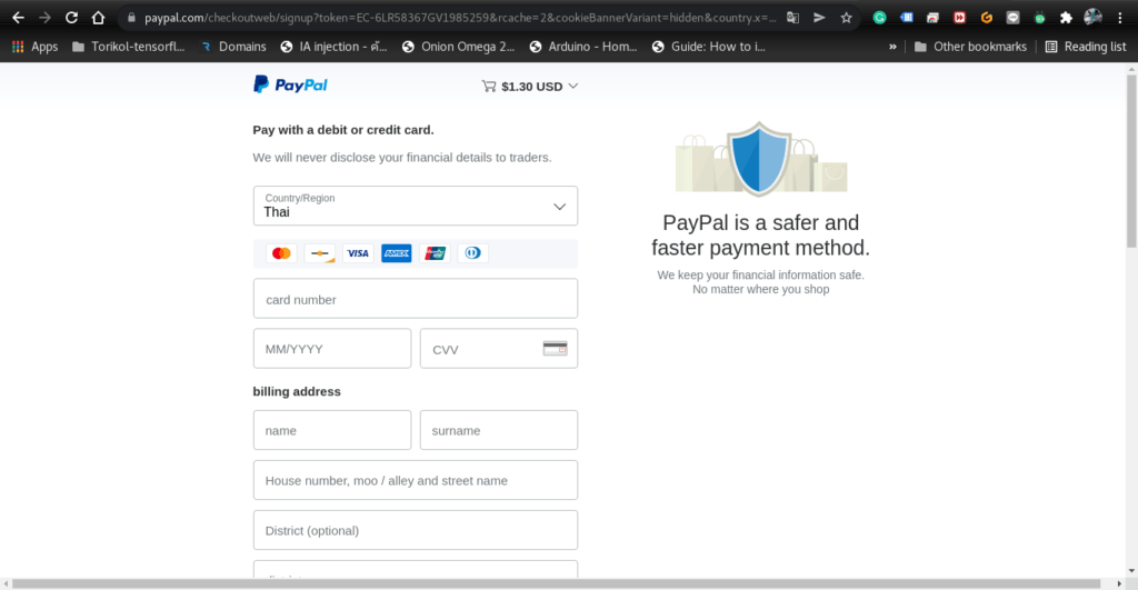
At this moment in time, only two payment options are supported, Paypal ( as well as Debit and Credit cards) and Direct Bank Transfer. I believe more options will be made available in future..
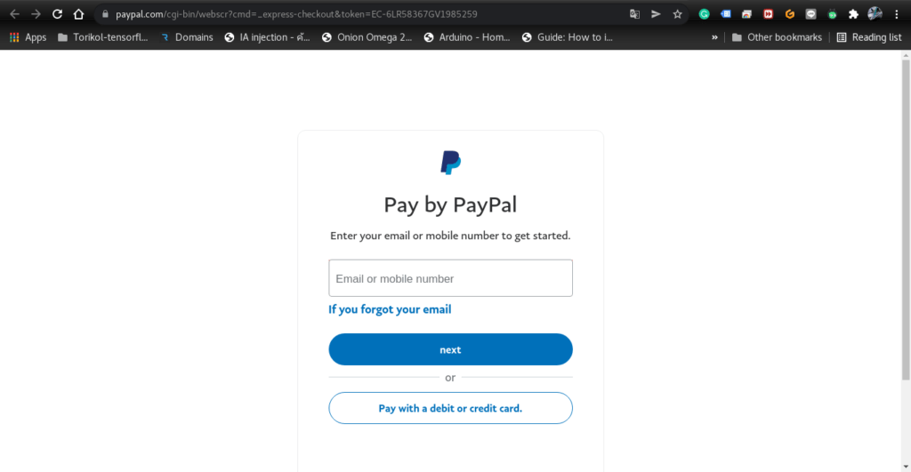
In my case, I chose Paypal and paid by Debit card.
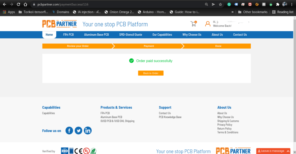
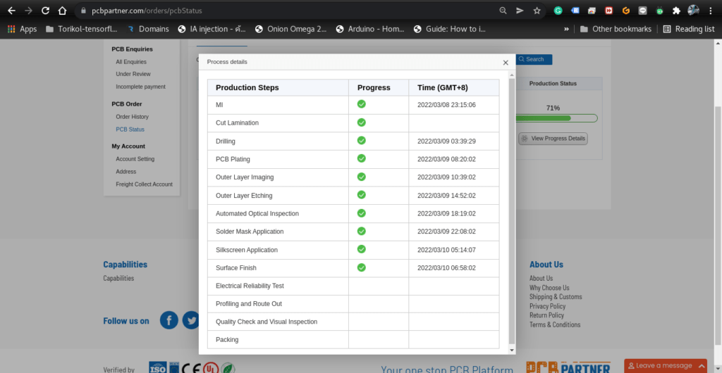
After payment was made successfully, you can also check on the status of your order…
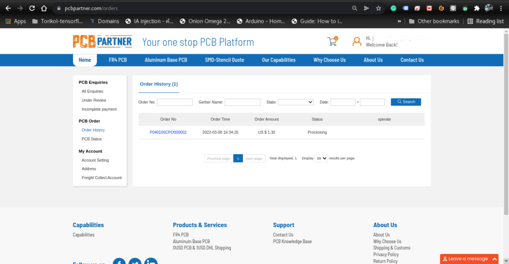
You can also review your order at any stage before or after payment, as well as get progress reports of the manufacturing process.
In conclusion, I would like to say that it was quite easy to order and make payment. The Website is easy to use, and everything is clear and easy to understand. The PCB was well manufactured and seems to be quite good quality