

These days, we are used to buying electronics components in chip (IC) form. There are however times (especially now with the huge logistics delays due to COVID-19, or the discontinuation of many DIP (Through-Hole-Type Dual Inline Package) IC’s by the manufacturers in favor of the smaller and cheaper to manufacture Surface-Mount type chips), that you may be tempted to construct your own logical gates from scratch.
Surface-Mount chips are quite easy to handle to a well-equipped maker, but the beginner often struggles to use these small components. It is also getting increasingly difficult to get hold of chips in DIP packaging. These are all situations where these circuits will definitely come in very handy
As part of a planned series on Logic Circuits and their extremely useful and versatile functionality, I decided to start off by showing you how many of these logic gates are build at the circuit level. My schematics are based on TTL levels (0v-0.8v is a Logic 0, and 2v-5v is a Logic 1).
In the following series of schematics, I will introduce you to the various logic gates ( BUFFER, NOT, AND, NAND, OR, NOR), as well as show you how to build them from scratch using nothing more than a few transistors and resistors, both of which seems to still be extremely easy to get hold of. The circuit(s) will also help you understand how they work, and that is also a great help to any beginner…
Let us start…
Our First circuit will be the BUFFER. This circuit is basically used as a logic amplifier. It’s use is to amplify a logic signal, strengthening the signal, without changing the state of the signal. In other words, it won’t change a logic 1 to a logic 0, or vice versa…
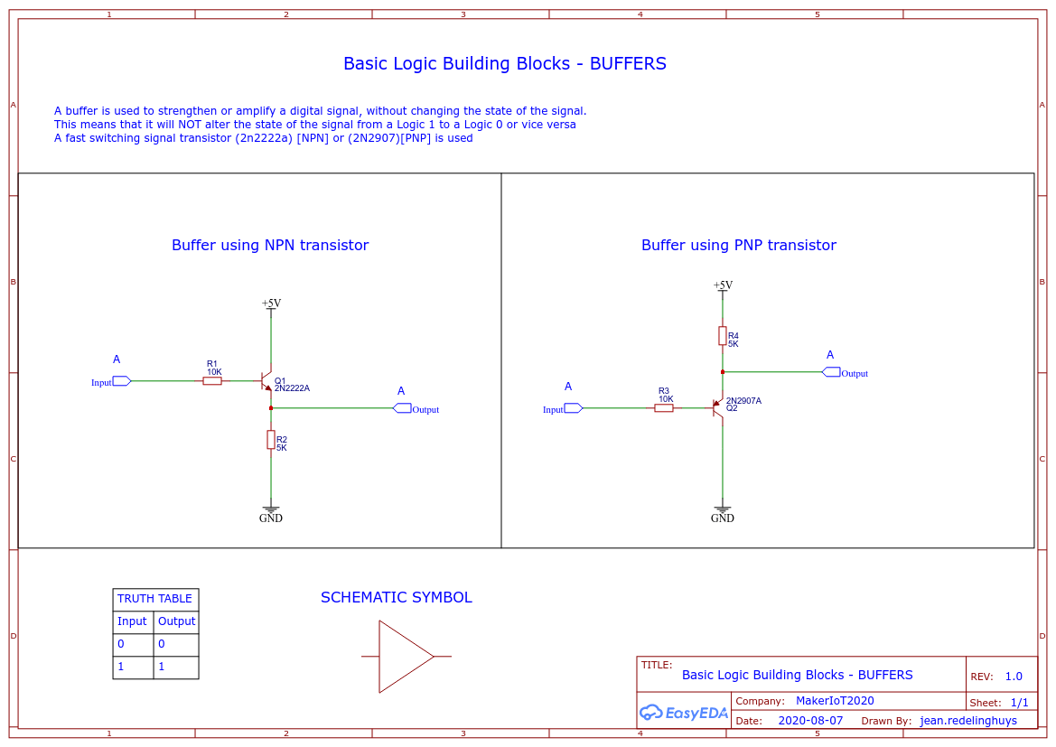
As you can see, the circuit is extremely easy to understand, but for clarity sake, I will explain it to you. Similar principles will apply to all the other circuits following below…In the NPN based buffer, transistor Q1 will remain off, keeping output A at logic 0 if input A is at a logic 0, and conduct (switch on), changing output A to a logic 1 if input 1 is at logic 1. The presence of a 5v signal at input A makes this happen.In our PNP model, output A is pulled up to 5v by resistor R4. It will thus be at logic 1 if a 5v signal is present at input A. If we were to pull input A to ground, making it logic 0, the transistor will conduct (switch on) and pull output 1 to ground, turning it into a logic 0!
Easy right?
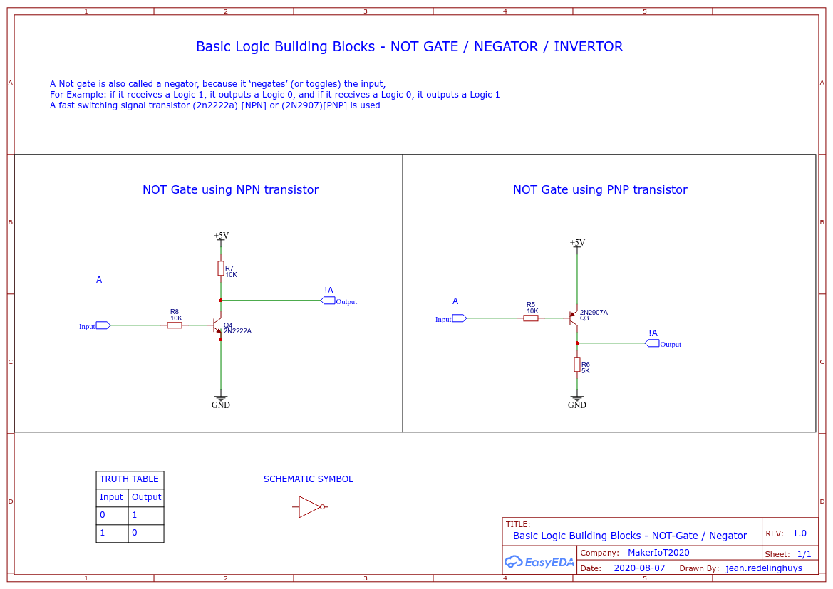
Our next circuit will be the NOT gate or negator or also sometimes called an inverter… This circuit will toggle the input and output, turning a logic 0 into a logic 1 and a logic 1 into a logic 0 respectively.
The AND gate is our next circuit. This gate operates by requiring that both of its inputs are at a logic 1 before the output will be changed to a logic 1 as well…
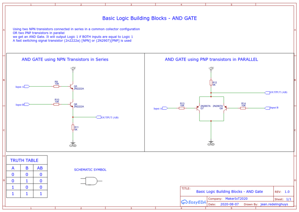
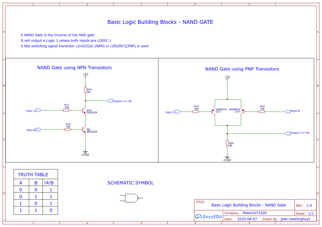
You will see that we require two transistors per gate to make the AND gate. AND gates with more inputs can be made as well, by simply adding more transistors in a similar configuration.The inverse of the AND gate is the NAND gate. This gate can also be constructed by placing a NOT gate at its output, effectively achieving the same result, but that makes it necessary to add another transistor and two resistors to the circuit. It is much more efficient to do it using only two transistors and 4 resistors…
The NAND gate will always output a logic 1 unless both its inputs are at logic 1, in which case the output will go to logic 0
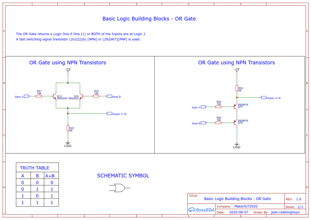
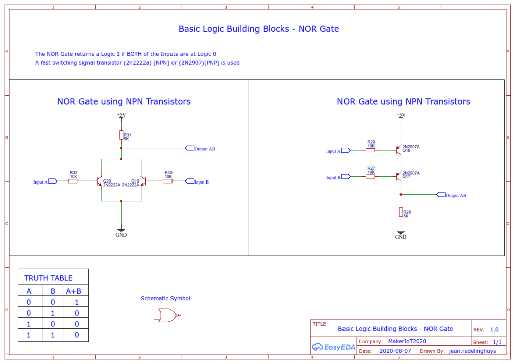
The OR and NOR gates will complete this short tutorial.
Their operation are similar, but inverse to each other.
The OR gate will output a logic 1 while one or both of its inputs are at logic 1, and a logic 0 when both inputs are at logic 0
The NOR gate will operate in a complementary way to the OR, meaning that it will output a logic 1 only if both inputs are at 0. Any other combination will cause it to output a logic 0.
We will not cover the XOR and XNOR gates today, these two deserve a lot of attention on their own, so that will be another tutorial…
You will now probably ask yourself, why should you know or even care about these circuits? They are as old as the mountains, and we don’t use them anymore… or do we ? Yes we still do. they are the building blocks of every digital circuit that you own and use every day, including your computer and smartphone. By combining these circuits in certain configurations, either with themselves, or with other logic gates, we can create extremely useful little circuits, from something as simple as an led flasher, tone generator, logic tester to as complex as a shift register with a memory function as well as a PWM controller circuit. The most interesting part of this is that all these circuits can be constructed without the need of a micro controller like an Arduino or a PIC…
In the next part of this series, I will start to show you some of these circuits…